In the vast realm of electronics, transistors serve as the unsung heroes, powering countless devices and circuits that have become an integral part of our daily lives. Among them, the 2N5551 NPN transistor stands out as a versatile and widely - utilized component. With its unique combination of features, it has carved a niche for itself in various applications, from the small - scale circuits within consumer electronics to the more complex systems in industrial and communication setups. This article delves deep into the world of the 2N5551, exploring its distinctive features, diverse applications, crucial datasheet details, and fundamental pinout configurations. Whether you're an electronics enthusiast, a student, or a professional engineer, understanding the 2N5551 can open up new possibilities in circuit design and innovation.
Comprehensive Overview of 2N5551 Transistor
The 2N5551 is a high-frequency, low-power NPN bipolar junction transistor (BJT) widely used in amplification, switching, and oscillation circuits. Its core advantages include excellent high-frequency response, low saturation voltage, and minimal power loss, making it ideal for small to medium-power electronic devices. Key applications span high-frequency signal amplification, pulse circuit switching, and low-power driving. With robust performance metrics—such as high breakdown voltages (Vce ≥ 150V), a DC current gain (hFE) of 80-250, and a characteristic frequency (fT) ≥ 100MHz—it balances reliability and efficiency, solidifying its role as a staple in electronic design.
2N5551 Transistor CAD Model
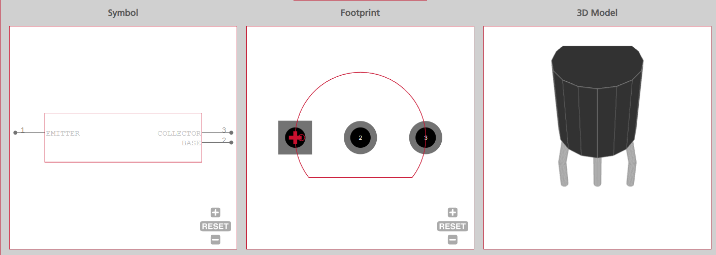
Pin Configuration of 2N5551 Transistor
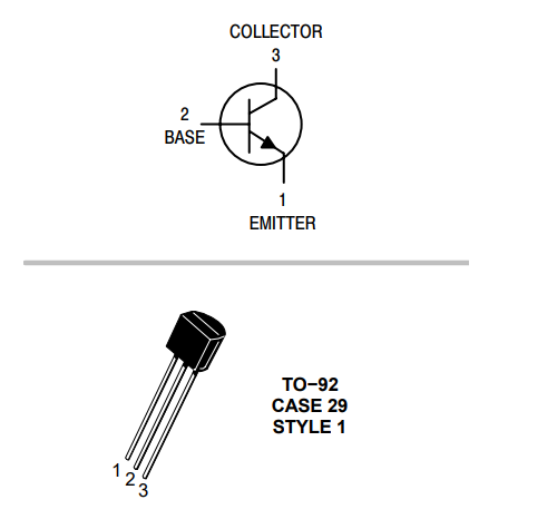
The 2N5551 transistor features a clear pin configuration, critical for proper circuit integration. In the common TO-92 package, three pins serve distinct roles: Pin 1 is the Emitter (E), the current outflow terminal typically connected to ground or low potential; Pin 2 acts as the Base (B), controlling collector-emitter current via base current (Ib); Pin 3 functions as the Collector (C), the current inflow terminal linked to loads or high potentials.
| Pin Number | Pin Name | Function Description |
|---|---|---|
| 1 | Emitter (E) | Emitter, the current outflow terminal, usually grounded or connected to a low potential |
| 2 | Base (B) | Base, which regulates the collector-emitter current (Ic) through the control current (Ib) |
| 3 | Collector (C) | Collector, the current inflow terminal, connected to the load or high potential terminal |
Characteristics and Technical Specifications of 2N5551 Transistor
Core Electrical Characteristics
- DC Characteristics:
- Collector-Base Breakdown Voltage (Vcb): ≥160V
- Collector-Emitter Breakdown Voltage (Vce): ≥150V
- Emitter-Base Breakdown Voltage (Veb): ≥6V
- DC Current Gain (hFE): 80-250 (at Ic=10mA, Vce=10V)
- High-Frequency Characteristics:
- Characteristic Frequency (fT): ≥100MHz (at Ic=10mA, Vce=20V)
- Output Capacitance (Cob): ≤15pF (at Vcb=10V, f=1MHz)
- Power and Temperature Characteristics:
- Maximum Collector Dissipation Power (Pc): 0.625W (at Tamb=25℃)
- Operating Junction Temperature Range (Tj): -55℃~+150℃
- Storage Temperature Range (Tstg): -55℃~+150℃
Limit Parameters (Absolute Maximum Values)
| Parameter | Value |
|---|---|
| Maximum Collector Current (Ic) | 0.6A |
| Maximum Base Current (Ib) | 0.1A |
| Junction Temperature (Tj) | 150℃ |
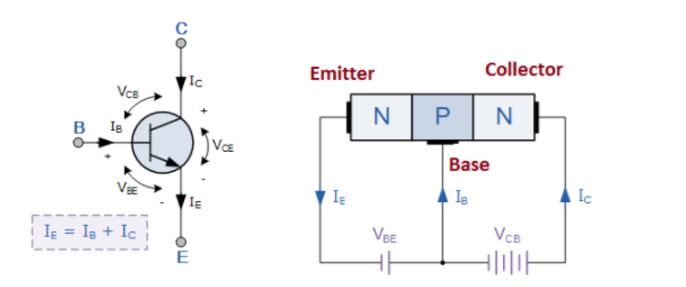
Circuit Diagram with 2N5551 NPN Transistor
2N5551 Features
Strong voltage resistance performance: The collector-emitter breakdown voltage (Vce) is ≥150V, and the collector-base breakdown voltage (Vcb) is ≥160V, enabling stable operation in relatively high-voltage environments and expanding the scope of application.
Stable current gain: Under the conditions of Ic=10mA and Vce=10V, the DC current gain (hFE) ranges from 80 to 250, ensuring reliable amplification performance and the stability of signal amplification.
Excellent high-frequency characteristics: The characteristic frequency (fT) is ≥100MHz (at Ic=10mA and Vce=20V), making it suitable for high-frequency application scenarios such as high-frequency signal amplification and oscillation.
Good power and temperature adaptability: The maximum collector dissipation power reaches 0.625W (at 25℃), and the operating junction temperature range is -55℃~+150℃, allowing stable operation in a relatively wide temperature range and power range.
Low output capacitance: The output capacitance (Cob) is ≤15pF (at Vcb=10V and f=1MHz), which reduces high-frequency signal loss and improves high-frequency response effects.
Excellent switching characteristics: It has a low saturation voltage, and can achieve fast switching after optimized design, making it suitable for switching applications such as pulse circuits and load driving.
2N5551 Applications
The 2N5551 is an NPN-type small-signal silicon transistor, featuring high-frequency response (typical characteristic frequency fT of 100MHz), medium power handling capability (maximum collector power dissipation of 625mW), and moderate current driving capacity (maximum collector current of 600mA). Its application scenarios mainly focus on "small-signal processing" and "low-power switching", with the following key applications:
Small-signal amplification circuits
As a core amplifying device, it is used in audio pre-amplification (such as signal preprocessing for small audio systems and headphone drivers), radio frequency (RF) signal amplification (such as amplifying weak signals at the receiving end of radios and walkie-talkies), and sensor signal amplification (such as amplifying weak electrical signals output by photoresistors and thermistors to adapt to subsequent AD sampling). Its high-frequency characteristics can reduce signal distortion, making it suitable for processing high-frequency, small-amplitude signals.
Low-power switch control
It acts as an electronic switch in small-current load scenarios, such as LED on/off control (controlling the on/off of collector current through base signals to drive low-power LEDs), small relay coil driving (needing to be paired with current-limiting resistors to control the relay's activation/deactivation for switching peripheral circuits), and logic level switching in digital circuits (adapting to the signal on/off requirements of TTL/CMOS circuits).
High-frequency oscillation and signal generation
Leveraging its high-frequency response capability, it is used in high-frequency oscillator circuits (such as LC oscillation circuits, generating sinusoidal signals in the radio frequency range for applications like remote control modules and carrier generation in small communication devices) and signal modulation circuits (assisting in implementing amplitude modulation or frequency modulation, commonly seen in simple wireless transmission equipment).
Pulse signal amplification and shaping
In digital systems or timing control circuits, it amplifies weak pulse signals (such as amplification of timer output signals) or shapes distorted pulse waveforms through its switching characteristics (such as eliminating signal jitter to output regular high-low level pulses, adapting to the triggering requirements of subsequent logic circuits).
Constant current sources and biasing circuits
Utilizing the transistor's current control characteristics, it constructs low-power constant current sources (such as providing stable operating current for low-power sensors and operational amplifiers) or serves as biasing circuits for power devices (providing appropriate base bias voltage/current for high-power transistors to ensure they operate in a stable amplification region).
Safe Operation of the 2N5551 NPN Transistor
The 2N5551 NPN transistor, a staple in many electronic circuits, requires careful handling to ensure safe operation.
First and foremost, adhering to the Safe Operating Area (SOA) is crucial. The product of the collector - emitter voltage (VCE) and the collector current (IC) should not exceed the maximum collector dissipation power (PC), which is 0.625W at 25℃. In high - temperature environments, derating is necessary. For example, when the ambient temperature reaches 100℃, PC should be reduced to 0.3W. Exceeding these limits can lead to overheating and permanent damage.
During soldering, it's vital to keep the temperature at or below 260℃ and the soldering time within 10 seconds. High temperatures can damage the delicate internal structure of the transistor. In applications involving high power, installing heat sinks is advisable to dissipate heat effectively and maintain a safe junction temperature.
Moreover, due to its ESD (Electro - Static Discharge) sensitivity level of Class 1A, anti - static measures such as using anti - static wrist straps and bags are essential during storage and handling to prevent damage from electrostatic charges.
Optimizing 2N5551 Transistor Efficiency and Performance
Amplification Circuit Optimization
In amplification circuits, the 2N5551's performance can be enhanced through meticulous biasing and impedance matching.
Biasing: Employing a voltage - divider biasing configuration, typically with resistors Rb1 and Rb2, helps stabilize the operating point of the transistor. Temperature variations can cause fluctuations in the transistor's DC current gain (hFE). But with proper voltage - divider biasing, the base voltage remains relatively constant, ensuring a stable collector current and minimizing gain variations. For instance, in an audio pre - amplification circuit, a stable operating point guarantees consistent sound amplification without distortion caused by hFE fluctuations.
Impedance Matching: Incorporating an LC (inductor - capacitor) network for impedance matching is crucial for high - frequency applications. The 2N5551 has a certain input and output impedance. By using an LC network, the impedance of the source and load can be matched to that of the transistor. This reduces signal reflections, which can cause power loss and distortion. As a result, the transistor can efficiently transfer power and amplify high - frequency signals, making it suitable for RF (radio frequency) amplification tasks.
Switching Circuit Optimization
For switching applications, the key lies in accelerating the switching speed and reducing power losses.
Accelerating Switching Speed: Connecting a small resistor (ranging from 100Ω - 1kΩ) in series with the base of the 2N5551 can suppress current overshoot during the turn - on process. Additionally, adding a capacitor (10pF - 100pF) in parallel with the base - emitter junction can speed up the turn - off process. When the transistor needs to switch off, the capacitor provides a path for the stored charge in the base region to discharge quickly, reducing the turn - off time. This is especially important in pulse - width modulation (PWM) circuits where rapid and accurate switching is required.
Reducing Power Losses: Avoiding over - driving the transistor is essential for minimizing power losses. Over - driving can lead to excessive saturation, increasing the turn - off delay and causing higher power dissipation during the transition between on and off states. By precisely controlling the base current, the transistor can operate at an optimal saturation level, reducing both conduction and switching losses. In a motor - driving circuit, this optimization ensures that the 2N5551 can switch the motor current efficiently, improving the overall system's energy efficiency.
Simulation Graph to 2N5551
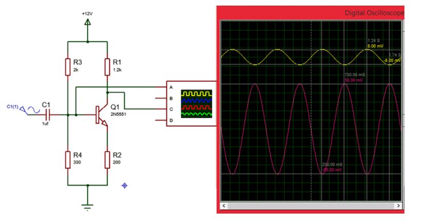
This simulation showcases a common - emitter amplifier built with a 2N5551 NPN transistor. The circuit on the left uses resistors R3 (2kΩ), R4 (330Ω) for voltage - dividing biasing, setting the base voltage to establish a proper operating point. R1 (1.2kΩ) and R2 (200Ω) act as collector and emitter resistors, respectively, determining the output impedance and current - voltage characteristics. C1 (1μF) is a coupling capacitor, allowing AC signals to pass while blocking DC.
The oscilloscope on the right displays two key waveforms. The upper yellow trace represents the input AC signal, likely a low - amplitude sinusoid. The lower pink waveform is the output, amplified by the 2N5551. Notice the significant gain: the output amplitude is much larger, demonstrating the transistor’s voltage amplification capability in this configuration. The smooth sinusoidal shapes indicate minimal distortion, showing the 2N5551 can effectively amplify AC signals for analog applications like audio pre - amplification, validating its use in linear amplification circuits.
Alternatives to the 2N5551 Transistor
| Part Number | Description | Manufacturer |
| 2N5551D26Z | Small Signal Bipolar Transistor, 0.6A I(C), 160V V(BR)CEO, 1-Element, NPN, Silicon, TO-92 | Fairchild |
| 2N5551TRE | Small Signal Bipolar Transistor, 160V V(BR)CEO, 1-Element, NPN, Silicon, TO-92 | Central |
| 2N5551RL1G | Small Signal NPN Bipolar Transistor, TO-92 (TO-226) 5.33mm Body Height, 2000-REEL | ON |
| 2N5551RLA | 600mA, 160V, NPN, Si, SMALL SIGNAL TRANSISTOR, TO-92, CASE 29-11, TO-226AA, 3 PIN | Rochester |
| 2N5551-AMMO | TRANSISTOR 600 mA, 160 V, NPN, Si, SMALL SIGNAL TRANSISTOR, TO-92, BIP General Purpose Small Signal | NXP |
| 2N5551LRM | 600mA, 160V, NPN, Si, SMALL SIGNAL TRANSISTOR, TO-92, CASE 29-11, TO-226AA, 3 PIN | Rochester |
| 2N5551LRP | Small Signal Bipolar Transistor, 0.6A I(C), 160V V(BR)CEO, 1-Element, NPN, Silicon, TO-92 | Motorola |
| 2N5551STOB | Small Signal Bipolar Transistor, 0.6A I(C), 160V V(BR)CEO, 1-Element, NPN, Silicon, TO-92 STYLE, E-LINE PACKAGE-3 | Diodes |
| 2N5551-AP | Small Signal Bipolar Transistor, 0.6A I(C), 160V V(BR)CEO, 1-Element, NPN, Silicon, TO-92, ROHS COMPLIANT, PLASTIC PACKAGE-3 | Micro |
| 2N5551L | Small Signal Bipolar Transistor, 0.6A I(C), 160V V(BR)CEO, 1-Element, NPN, Silicon, TO-92 STYLE, E-LINE PACKAGE-3 | Diodes |
Package Dimensions of 2N5551
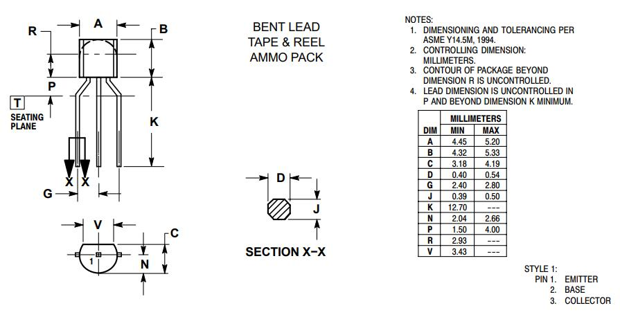
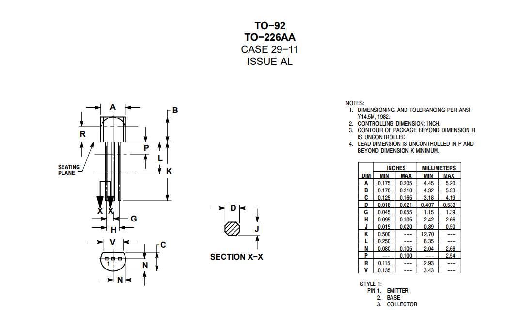
TO-92: It is a plastic through-hole package, very suitable for manual soldering, and widely used in the consumer electronics field.
SOT-23: It is a surface-mount package, and its small size makes it suitable for high-density PCB design.
Key Dimension Parameters (TO-92 Package)
Parameter | Value Range |
|---|---|
Pin Pitch | 2.54mm (standard) |
Package Length | 4.9mm-5.2mm |
Pin Length | 3.0mm-4.0mm |
Conclusion
As a high-performance NPN transistor, the 2N5551 has been widely used in amplification, switching, and high-frequency circuits due to its advantages of high voltage resistance, high-frequency characteristics, and low cost. During the design process, attention should be paid to its safe operating area, heat dissipation conditions, and parameter matching, and simulation tools should be used to optimize circuit performance. By reasonably selecting alternative models and complementary transistors, its application scenarios can be further expanded to meet diverse design needs.


 Wishlist (0 Items)