In the field of modern electronic technology, CMOS (Complementary Metal-Oxide-Semiconductor) integrated circuits have become core components in digital and analog circuit design due to their low power consumption, high integration, and excellent compatibility. As a classic CMOS device, the CD4007 occupies an important position in electronic engineering practice with its unique structural design and flexible application characteristics. This article will comprehensively analyze the technical details and practical value of this integrated circuit from multiple dimensions such as structure, characteristics, and applications.
What is CD4007?
The CD4007 is a versatile integrated circuit (IC) belonging to the CMOS (Complementary Metal-Oxide-Semiconductor) family, widely used in electronics for its flexible transistor configuration. At its core, it contains three pairs of complementary MOS transistors: each pair consists of one N-channel MOSFET (NMOS) and one P-channel MOSFET (PMOS). This structure allows designers to configure the transistors in various ways—such as in series, parallel, or as individual devices—to suit different circuit needs, from simple switches and inverters to more complex logic gates or amplifiers. A key advantage of the CD4007 is its compatibility with multiple logic families, including TTL (Transistor-Transistor Logic) and NMOS, making it adaptable to diverse system designs. It operates over a wide voltage range (typically 3V to 18V), offers low power consumption, and exhibits good noise immunity, which is crucial for maintaining signal integrity in sensitive applications. Additionally, the IC includes built-in protection against electrostatic discharge (ESD) via clamping diodes between the drain terminals and ground, enhancing its durability during handling and operation. These features, combined with its flexibility and cost-effectiveness, make the CD4007 a staple in educational projects, prototyping, and practical electronic designs.
Core Structure and Working Principle of CD4007
The core advantage of CD4007 stems from its sophisticated internal transistor configuration. The chip contains three pairs of complementary enhancement-mode MOS transistors — each pair consists of one N-channel (NMOS) and one P-channel (PMOS) transistor, totaling 3 NMOS transistors and 3 PMOS transistors. This symmetrical structure allows it to operate in both series and parallel modes, laying the foundation for diverse circuit designs.
In terms of electrical principles, the operation of CD4007 relies on the switching characteristics of MOS transistors. When a high voltage is applied to the gate of an NMOS transistor, a conductive channel is formed between the drain and the source, turning the transistor on; while a PMOS transistor turns on when a low voltage is applied to its gate. By controlling the gate voltage, precise switching control of the transistors can be achieved, thereby constructing various logic functions or signal processing circuits.
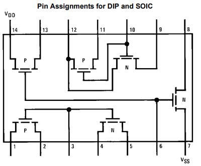
It is worth noting that the substrates of all PMOS transistors inside the chip are connected to the positive power supply pin (VDD, pin 14), and the substrates of NMOS transistors are uniformly connected to the ground (VSS, pin 7). This design ensures that the transistors work in a stable bias state and reduces the interference of the substrate effect on circuit performance.
Specifications of CD4007
| Type | Parameter | Value |
|---|---|---|
| Mount | Mounting Type | Surface Mount |
| Package / Case | 14-SOIC (0.154, 3.90mm Width) | |
| Number of Pins | 14 | |
| Supplier Device Package | 14-SOIC | |
| Operating Conditions | Operating Temperature | -40°C to 85°C |
| Max Operating Temperature | 85°C | |
| Min Operating Temperature | -40°C | |
| Electrical Characteristics | Supply Voltage | 3V to 15V |
| Max Supply Voltage | 15V | |
| Min Supply Voltage | 3V | |
| Propagation Delay | 50 ns | |
| Design Specifications | Series | 4000B |
| Logic Function | Inverter | |
| Logic Type | Complementary Pair Plus Inverter | |
| Number of Circuits | 2 | |
| Number of Bits | 3 | |
| Number of Input Lines | 3 | |
| Number of Output Lines | 3 | |
| Base Part Number | 4007 | |
| Polarity | Inverting | |
| Additional Details | Packaging | Tube |
| Part Status | Obsolete | |
| Moisture Sensitivity Level (MSL) | 1 (Unlimited) | |
| RoHS Status | RoHS Compliant | |
| Lead Free | Lead Free | |
| Published | 1999 |
Features of CD4007
| Feature | Description |
|---|---|
| Wide supply voltage range | 3.0V to 15V |
| High noise immunity | 0.45 VCC (Typ.) |
| Quiescent current testing | 100% tested at 20V |
| Symmetrical output characteristics | Standardized, ensuring reliable output |
Transistor Configuration: It consists of three pairs of complementary MOS transistors—specifically, three N-channel MOSFETs (NMOS) and three P-channel MOSFETs (PMOS). This pairing allows flexible circuit design by enabling series, parallel, or other custom configurations of the transistors.
Wide Voltage Range: Operates over a broad supply voltage range, typically from 3V to 18V. This flexibility makes it compatible with various power sources and suitable for both low-voltage and moderate-voltage applications.
Low Power Consumption: As a CMOS device, it exhibits very low static power dissipation, making it ideal for battery-powered devices or circuits where energy efficiency is critical.
High Noise Immunity: CMOS technology inherently provides strong noise immunity, ensuring stable operation even in environments with electrical interference. This feature enhances the reliability of circuits using the CD4007.
ESD Protection: Includes built-in electrostatic discharge (ESD) protection mechanisms, such as clamping diodes between terminals and ground. These protect the IC from damage during handling or operation in static-prone environments.
Compatibility: Interfaces seamlessly with different logic families, including TTL (Transistor-Transistor Logic), NMOS, and other CMOS devices. This versatility simplifies integration into mixed-logic systems.
Flexibility in Applications: Due to its configurable transistor pairs, it can be used for a wide range of purposes, such as constructing inverters, amplifiers, oscillators, voltage regulators, logic gates, and even simple analog circuits. This adaptability makes it a popular choice for prototyping and educational projects.
Temperature Tolerance: Functions reliably across a typical temperature range of -55°C to 125°C (industrial grade), ensuring performance in harsh or varying thermal conditions.
CD4007 Pin Configuration

| Pin No | Pin Name | Description |
|---|---|---|
| 1 | 2Dp | The drain of p Channel 2 |
| 2 | 2Sp | Source of p Channel 2 |
| 3 | 2A | Input Channel 2 |
| 4 | 2Sn | Source of n Channel 2 |
| 5 | 2Dn | The drain of n Channel 2 |
| 6 | 1A | Input Channel 1 |
| 7 | VSS | Source Supply |
| 8 | 1Dn | The drain of n Channel 1 |
| 9 | 3Sn | Source of n Channel 3 |
| 10 | 3A | Input Channel 3 |
| 11 | 3Sp | Source of p Channel 3 |
| 12 | 3Y | Output |
| 13 | 1Dp | The drain of p Channel 1 |
| 14 | VDD | Drain Supply |
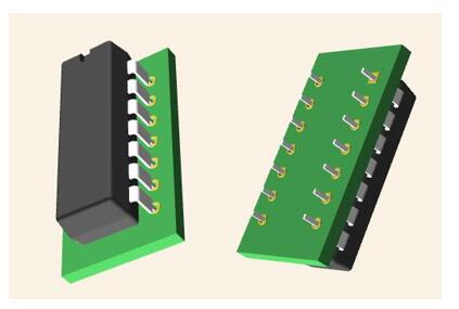
CD4007 CAD Model

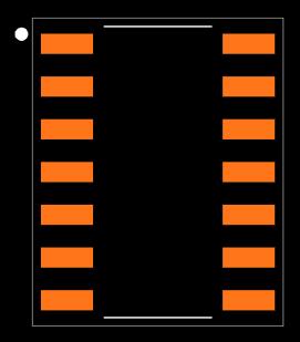
CD4007 Footprint

CD4007 CAD Model
Applications of CD4007
Digital Logic Circuits
Inverters: By combining one N-channel and one P-channel transistor from a pair, the CD4007 can function as a NOT gate (inverter), a fundamental building block of digital logic.
Logic Gates: Configuring multiple transistor pairs allows the creation of complex gates like AND, OR, NAND, and NOR, enabling basic digital logic operations.
Flip-Flops and Latches: With proper wiring, it can form simple memory elements (e.g., SR flip-flops) for storing binary data in sequential logic circuits.
Analog Circuits
Amplifiers: When configured as a complementary pair (push-pull amplifier), it can amplify low-power analog signals, such as audio or sensor outputs.
Oscillators: By leveraging its transistor pairs with capacitors and resistors, it can generate oscillating signals (e.g., square waves) for timing or clock applications.
Voltage Regulators: In shunt configurations, it can stabilize voltage levels, protecting sensitive components from voltage fluctuations.
Threshold Detectors: It can act as a comparator to detect when an input voltage crosses a predefined threshold, useful in sensor-based systems.
Power Management
Voltage Level Shifters: Its compatibility with CMOS, NMOS, and TTL logic families allows it to convert signals between different voltage levels (e.g., 5V to 12V), facilitating communication between mismatched devices.
Low-Power Switches: As MOSFETs consume minimal power in the "on" state, it can act as a low-loss switch to control power flow in battery-operated devices.
Educational and Prototyping
Due to its transparency (exposing individual transistors) and flexibility, it is widely used in electronics education to teach circuit design, transistor behavior, and logic principles. It simplifies prototyping of custom circuits without requiring specialized ICs.
Specialized Uses
ESD Protection Modules: Its built-in clamping diodes can be repurposed to protect other components in a circuit from electrostatic discharge.
Light Sensors: When paired with a light-dependent resistor (LDR), it can form simple light-sensing circuits (e.g., automatic nightlights).
Parts with Similar Specs of CD4007
| Part Number | Manufacturer | Package / Case | Number of Pins | Propagation Delay | Min Supply Voltage | Supply Voltage |
|---|---|---|---|---|---|---|
| CD4007CM | ON Semiconductor | 14-SOIC (0.154, 3.90mm Width) | 14 | 50 ns | 3 V | 3V ~ 15V |
| MC14007UBD | ON Semiconductor | 14-SOIC (0.154, 3.90mm Width) | 14 | 18 ns | - | 5 V |
| SN74HCT04DR | Texas Instruments | 14-SOIC (0.154, 3.90mm Width) | 14 | 55 ns | 3 V | 3V ~ 18V |
Manufacturer of CD4007
The main manufacturer of CD4007 is Texas Instruments (TI). Many CD4007 - related products, such as CD4007UB, CD4007UBEG4 and CD4007UBNSRG4, are all produced by Texas Instruments. Texas Instruments is a well - known semiconductor company, and its CD4007 products have the characteristics of high - quality and stable performance, which are widely used in various electronic circuits. In the past, Fairchild (now onsemi) also produced CD4007, but some of its models may have been discontinued. Overall, Texas Instruments is the leading manufacturer in the current CD4007 market.
The CD4007 demonstrates the remarkable adaptability of CMOS technology through its distinctive transistor array structure, wide voltage operating range, and flexible configuration options. From simple logic gates to intricate signal processing circuits, this IC plays a crucial role in electronics education, prototype development, and small-scale applications. For electronic engineers and hobbyists alike, a deep understanding of the CD4007's working principles and application techniques not only broadens circuit design perspectives but also embodies the electronic design philosophy of "controlling complexity with simplicity"—building infinitely possible electronic systems with the most fundamental components.
CD4007 Datasheet PDF
Hot-selling products of SIC
71421LA55J8 UPD44165184BF5-E40-EQ3-A SST39VF800A-70-4C-B3KE IS66WV1M16DBLL-55BLI-TR AS4C32M16SB-7BIN W25Q16FWSNIG
AS7C34098A-20JIN 752369-581-C W957D6HBCX7I TR IS61LPS12836EC-200B3LI MX25L12875FMI-10G QG82915PL
Product information is from SIC Electronics Limited. If you are interested in the product or need product parameters, you can contact us online at any time or send us an email: sales@sic-chip.com.


 Wishlist (0 Items)