

- RFQ
- BOM
-
Contact Us
Tel: +86-0755-83501315
Email: sales@sic-components.com


- Chinese
- English
- French
- German
- Portuguese
- Spanish
- Russian
- Japanese
- Korean
- Arabic
- Irish
- Greek
- Turkish
- Italian
- Danish
- Romanian
- Indonesian
- Czech
- Afrikaans
- Swedish
- Polish
- Basque
- Catalan
- Esperanto
- Hindi
- Lao
- Albanian
- Amharic
- Armenian
- Azerbaijani
- Belarusian
- Bengali
- Bosnian
- Bulgarian
- Cebuano
- Chichewa
- Corsican
- Croatian
- Dutch
- Estonian
- Filipino
- Finnish
- Frisian
- Galician
- Georgian
- Gujarati
- Haitian
- Hausa
- Hawaiian
- Hebrew
- Hmong
- Hungarian
- Icelandic
- Igbo
- Javanese
- Kannada
- Kazakh
- Khmer
- Kurdish
- Kyrgyz
- Latin
- Latvian
- Lithuanian
- Luxembou..
- Macedonian
- Malagasy
- Malay
- Malayalam
- Maltese
- Maori
- Marathi
- Mongolian
- Burmese
- Nepali
- Norwegian
- Pashto
- Persian
- Punjabi
- Serbian
- Sesotho
- Sinhala
- Slovak
- Slovenian
- Somali
- Samoan
- Scots Gaelic
- Shona
- Sindhi
- Sundanese
- Swahili
- Tajik
- Tamil
- Telugu
- Thai
- Ukrainian
- Urdu
- Uzbek
- Vietnamese
- Welsh
- Xhosa
- Yiddish
- Yoruba
- Zulu
- Kinyarwanda
- Tatar
- Oriya
- Turkmen
- Uyghur
- Tag List
- Comprehensive Analysis of P-Channel MOSFET: Structure, Working Principle, Application and Selection Guide
Comprehensive Analysis of P-Channel MOSFET: Structure, Working Principle, Application and Selection Guide
I. Basic Concepts and Core Characteristics of P-Channel MOSFET
1.1 Definition and Essence
The P-Channel Metal-Oxide-Semiconductor Field-Effect Transistor (P-Channel MOSFET) is a voltage-controlled semiconductor device. Its conductive channel is dominated by P-type carriers (holes). Different from the N-channel MOSFET, the P-channel device forms a conductive channel by applying a negative voltage to the gate (relative to the source), allowing current to flow from the source to the drain. Its core structure uses an N-type silicon substrate, with heavily doped P+ regions embedded on both sides as electrodes. The gate is isolated from the substrate by a silicon dioxide insulating layer, forming a typical three-layer structure of "metal-oxide-semiconductor".
1.2 Circuit Symbol and Physical Identification
The circuit symbol of the P-channel MOSFET has the following characteristics:
The arrow of the source (S) points outward, indicating that the current flows into the source (opposite to the inward arrow of the N-channel).
The connection between the drain (D) and the source: A dashed line represents the enhancement mode (default off state), and a solid line represents the depletion mode (default on state).
The direction of the body diode is from the drain to the source (opposite to the body diode direction of the N-channel).
1.3 Core Differences from N-Channel MOSFET
Characteristics P-Channel MOSFET N-Channel MOSFET
Conduction Condition Gate voltage is lower than the source voltage (VGS < VTH) Gate voltage is higher than the source voltage (VGS > VTH)
Carrier Type Holes (with a mobility approximately 1/3 of that of electrons) Electrons (with high mobility)
Typical RDS(on) Higher resistance under the same size (2 - 3 times larger) Low-resistance characteristic
Switching Speed Slower (suitable for scenarios below 100kHz) Faster (can reach the MHz level)
Circuit Position High-side switch (on the positive side of the power supply) Low-side switch (on the ground side)
II. Working Principle and Structural Analysis of P-Channel MOSFET
2.1 Working Mechanism of Enhancement-Mode P-Channel MOSFET
Off State (VGS ≥ 0V)
When the voltage difference between the gate and the source is zero or positive, no P-type channel is formed in the N-type substrate, and the source and the drain are isolated by the N-type material, so current cannot flow. At this time, the body diode is in the reverse-biased state, and the device is turned off.
Conduction Process (VGS < VTH)
Effect of Negative Gate Voltage: When a negative voltage is applied to the gate (e.g., VGS = -5V), the electric field formed between the gate and the substrate attracts the holes in the N-type substrate to gather under the gate.
Channel Inversion: The accumulated holes form a P-type conductive channel, connecting the source and the drain.
Current Flow: When a positive voltage is applied to the source, holes flow from the source to the drain through the channel, forming the drain current ID.
Working Regions
Linear Region: When VDS is small, ID has a linear relationship with VDS, and the device is equivalent to a variable resistor.
Saturation Region: When VDS ≥ |VGS - VTH|, the channel pinches off on the drain side, and ID is only determined by VGS. At this time, the device is equivalent to a current source.
2.2 Special Mechanism of Depletion-Mode P-Channel MOSFET
Default On State: During the manufacturing process, positive ions are implanted into the gate oxide layer, pre-inducing a P-type channel. The device is turned on without a gate voltage.
Turn-off Control: Applying a positive gate voltage (VGS > 0V) repels the holes, increasing the channel resistance until it reaches the pinch-off voltage VP and the device turns off.
Application Scenarios: Rarely used in switching circuits, mainly used as constant current sources or signal amplifiers in analog circuits.
2.3 Details of the Physical Structure
Substrate: N-type silicon base, and the doping concentration affects the threshold voltage VTH.
Source-Drain Region: Heavily doped P+ region (boron ion implantation) to reduce the contact resistance.
Oxide Layer: The thickness of the silicon dioxide layer under the gate is about 10 - 20nm, which determines the gate capacitance and breakdown voltage.
Body Connection: The substrate is usually internally connected to the source to avoid forward biasing of the PN junction.
III. Core Advantages and Application Scenarios of P-Channel MOSFET
3.1 Analysis of Technical Advantages
Simplification of High-side Switching
It can be directly connected in series between the positive pole of the power supply and the load without the need for a level-shifting circuit (for example, N-channel driving requires a bootstrap capacitor).
Typical application: In a lithium battery protection board, when the battery is connected in reverse, the body diode blocks the current. When connected correctly, the negative bias voltage on the gate turns the device on.
Low-power Drive Characteristics
The insulated gate structure gives it an input impedance as high as 10^12Ω, and the drive current is negligible (<1μA).
It is suitable for direct driving by microcontrollers (for example, a 3.3V logic level can meet the requirements of a device with VTH = -2V).
Reverse Polarity Protection
The body diode naturally has the function of preventing reverse connection, which is superior to the Schottky diode solution (the forward voltage drop is lower, such as 0.7V vs 0.3V).
When actively driven to conduct (e.g., VGS = -10V), RDS(on) can be as low as 20mΩ, reducing power consumption by more than 90% compared to the body diode.
3.2 Typical Application Fields
Battery Management System (BMS)
Charge and Discharge Control: Connected in series to the positive pole of the lithium battery, and the on-off is controlled by the negative pulse signal output by the MCU.
Overvoltage Protection: When the battery voltage exceeds 4.3V, the P-channel MOSFET is turned off to cut off the charging circuit.
Automotive Electronics
LED Lighting Drive: High-side dimming of automotive taillights, and the gate voltage is adjusted by PWM signals to control the brightness.
Wiper Motor Control: In the H-bridge circuit, the P-channel is responsible for high-side switching, and the N-channel is responsible for low-side switching to achieve forward and reverse rotation.
Consumer Electronics
Power Switching of Laptop Computers: When switching between the AC adapter and the battery, the P-channel MOSFET is used as a high-side switch to reduce power consumption.
Load Control of Mobile Power Supplies: When on standby, the P-channel device is turned off, reducing the quiescent current to below 1μA.
Industrial Control
Sensor Power Management: In the PLC system, the power supply of sensors is turned on or off as needed, extending the battery life of the 48V power supply system.
Soft Start of Motors: The P-channel MOSFET is driven by a ramp voltage to avoid inrush current during motor starting.
IV. Key Parameter Selection and Testing Methods for P-Channel MOSFET
4.1 Guide to Selecting Core Parameters
Drain-Source Breakdown Voltage (VDS)
It should be more than 1.5 times the maximum working voltage of the circuit (for example, select VDS ≥ 40V for a 24V system).
Consider the surge voltage (for example, select VDS ≥ 60V for automotive circuits to cope with cold start pulses).
Continuous Drain Current (ID)
The rated current should exceed 1.8 times the peak current of the load (for example, select ID ≥ 9A for a 5A load).
Pay attention to temperature derating (for example, the ID of the TO-220 package needs to be derated by 50% at 70°C).
On-resistance (RDS(on))
For low-power scenarios: RDS(on) < 100mΩ (such as for handheld devices).
For power applications: RDS(on) < 50mΩ (such as for motor drives, a heat sink is required).
Threshold Voltage (VTH)
For logic-level driving: Select VTH between -1.5V and -3V (suitable for 3.3V/5V MCUs).
For high-voltage applications: VTH = -5V to -10V (to reduce the risk of false triggering).
Gate Charge (QG)
For high-frequency switching (>50kHz): QG < 20nC.
For low-frequency applications: QG < 50nC is sufficient.
4.2 Multimeter Testing Process
Step 1: Discharge and Initial Detection
Short-circuit the G/S/D poles to eliminate residual charges.
Use the diode range to measure. The forward voltage drop from S to D should be 0.4 - 0.7V (the body diode is conducting), and it should be open circuit from D to S.
Step 2: Gate Control Test
Connect the black probe to the S pole and the red probe to the D pole. At this time, it should show an open circuit.
Touch the G pole briefly with the red probe (apply a negative voltage), and then measure the resistance from S to D again. It should be conductive (resistance < 100Ω).
After short-circuiting the G/S poles for discharge, the S to D should return to an open circuit. Otherwise, the device fails.
Step 3: Withstand Voltage Test
Use a megohmmeter to measure the insulation resistance between G and S, and between G and D. It should be > 100MΩ. Otherwise, the oxide layer is damaged.
V. Common Failure Modes and Protection Strategies of P-Channel MOSFET
5.1 Main Causes of Failure
Gate Overvoltage Breakdown
Electrostatic discharge (ESD) causes the oxide layer to break down (the typical withstand voltage is < 20V).
Manifestation: The resistance between the G-S poles drops to < 1kΩ, and the device remains continuously on or off.
Thermal Runaway
Overcurrent causes the junction temperature to exceed 150°C (for example, when RDS(on) = 100mΩ and ID = 3A, the power consumption is 9W, and a heat sink with RθJA < 16.7°C/W is required).
Appearance characteristics: The package cracks, and the pin solder joints melt.
Body Diode Burnout
When the power supply is connected in reverse, the body diode conducts continuously (for example, when a 12V power supply is connected in reverse, the body diode bears a 12V forward voltage, and the power consumption = 12V × 1A = 12W).
Protection: Connect a Schottky diode in parallel for current sharing (the rated current should be more than 2 times the load current).
5.2 Key Points of Protection Design
Gate Protection Circuit
Connect a 10 - 100Ω resistor in series to suppress switching spikes.
Connect a 15V voltage regulator diode in parallel (such as BZT52C15) to prevent transient overvoltage.
Heat Dissipation Design
Power calculation: Pd = ID² × RDS(on) + QG × VGS × f (switching loss).
Heat sink selection: RθJA < (Tj(max) - TA)/Pd (when Tj(max) = 150°C and TA = 25°C, RθJA < 125°C/Pd).
EMI Suppression
Connect a 100nF ceramic capacitor in parallel between the gate and the source (to reduce switching noise).
Connect a bead in series to the drain (100Ω/100MHz) to suppress high-frequency oscillations.
VI. Technological Development and Future Trends of P-Channel MOSFET
6.1 Application of Wide Bandgap Materials
SiC P-channel MOSFET: The breakdown field strength is 10 times that of silicon, enabling the realization of 1200V high-voltage devices (RDS(on) is 50% lower than that of silicon devices).
GaN HEMT compatible design: Integrate P-channel devices into gallium nitride power modules to simplify the high-side drive circuit.
6.2 Integration and Intelligence
Single-chip H-bridge: Integrate P-channel and N-channel MOSFETs into the same package (such as Infineon BTS7960, with RDS(on) of 43mΩ and a rated current of 40A).
Intelligent driver ICs: Built-in undervoltage lockout, overcurrent protection, and temperature monitoring (such as TI's DRV8833).
VII. Conclusion
With its unique high-side switching characteristics and simplified drive logic, the P-channel MOSFET plays an irreplaceable role in fields such as battery management, automotive electronics, and consumer electronics. Although it faces challenges such as higher on-resistance and slower switching speed, its advantages in reverse protection and low-power driving are still irreplaceable. With the development of wide bandgap semiconductor technology and the popularization of integrated drive solutions, P-channel MOSFETs will have more possibilities in high-voltage and high-frequency scenarios. In engineering applications, precise selection should be combined with load characteristics, and at the same time, heat management and overvoltage protection should be done well to give full play to their technical advantages and ensure system reliability.
https://www.sic-components.com/single-fets-mosfets

Hot Products
View More-

XW3A-P843-S026 Omron Automation and Safety
-
9456760000 Weidmüller
-
1516726 Phoenix Contact
-
1452851 Phoenix Contact
-
1155995 Phoenix Contact
-
1783530000 Weidmüller
-
1517291 Phoenix Contact
-
1452437 Phoenix Contact
-
XW3D-P855-G11 Omron Automation and Safety
-
DRT2-MD32ML Omron Automation and Safety
-
1202470039 Molex
-
1516234 Phoenix Contact
Related Blogs
-
2025 / 07 / 09
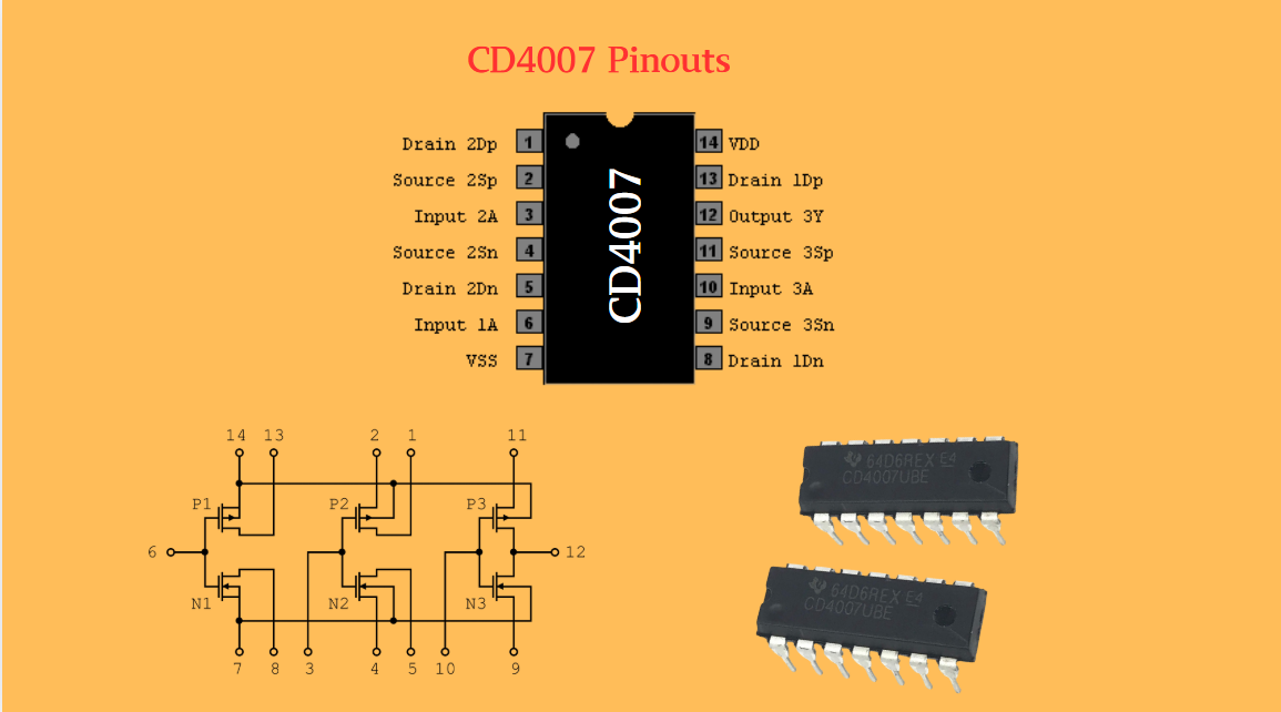
CD4007: A Comprehensive Analysis of a Multifunctional CMOS Integrated Circuit
In the field of modern electronic technology, CMOS (Complementary Metal-Oxide-Semiconductor) integrated circuits have become core components in digital and analog circuit design due to their low power consumption, high integration, and excellent compatibility. As a classic CMOS device, the CD4007 oc...
-
2025 / 07 / 07
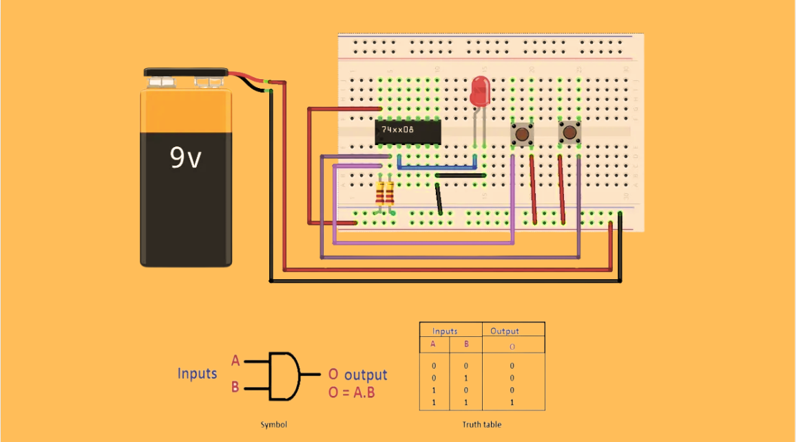
Understanding IC 7408: A Fundamental Component in Digital Logic Design
In the vast and intricate realm of digital electronics, integrated circuits (ICs) serve as the building blocks that enable the creation of complex and powerful systems. Among these, the IC 7408 holds a special place as a fundamental component in digital logic design. This article aims to provide a c...
-
2025 / 07 / 04
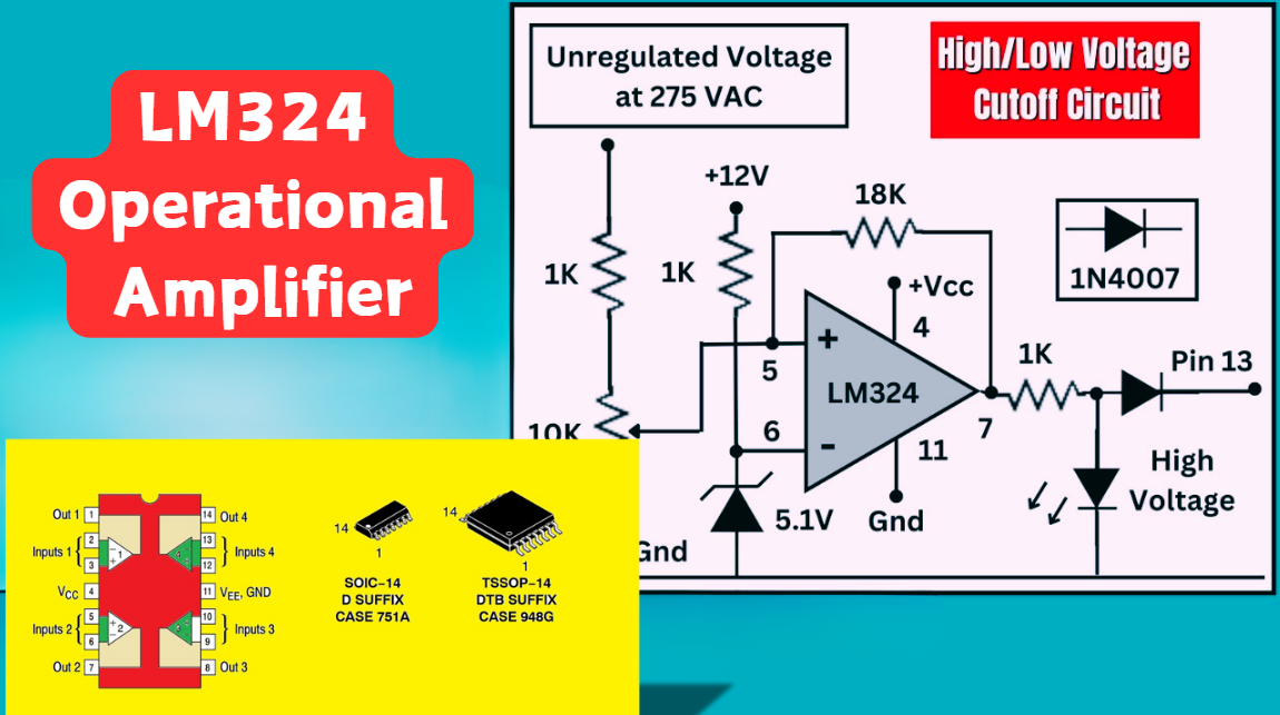
LM324 Operational Amplifier Comprehensive Guide: Pins, Applications, Packaging, and Datasheet
The LM324 is a low-cost integrated circuit featuring four independent operational amplifiers (op-amps), renowned for its wide voltage adaptability, low power consumption, and high reliability in industrial and consumer electronics. With a single-supply voltage range of 3V to 32V (or dual-supply rang...
-
2025 / 07 / 02
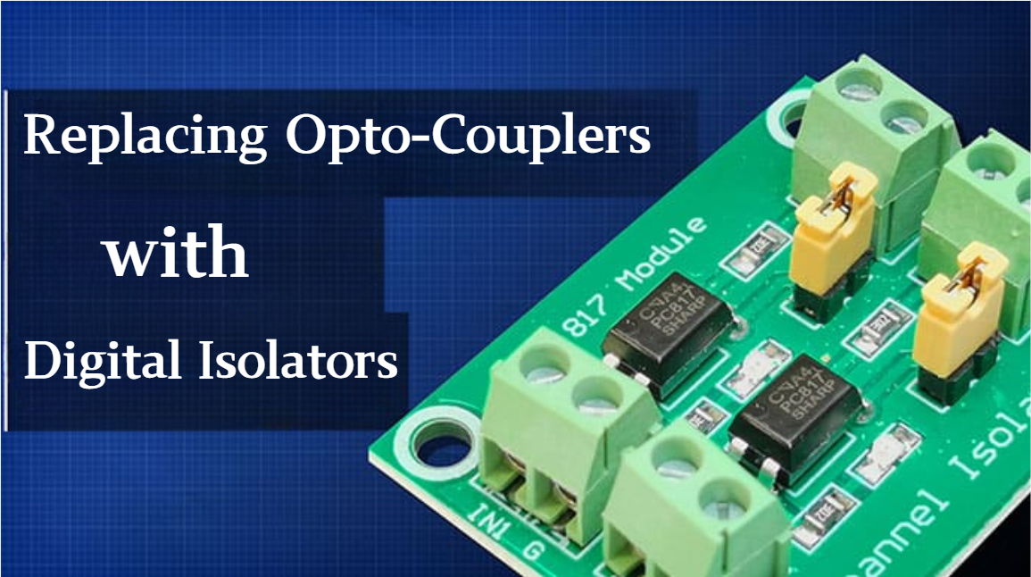
A Comprehensive Guide to Replacing Opto-Couplers with Digital Isolators: From Principles to Practice
In the ever-evolving landscape of electronic design, the transition from opto-couplers to digital isolators marks a pivotal shift in isolation technology. For decades, opto-couplers have been the cornerstone of electrical isolation in industrial control, medical devices, and power systems, relying o...
-
2025 / 06 / 30
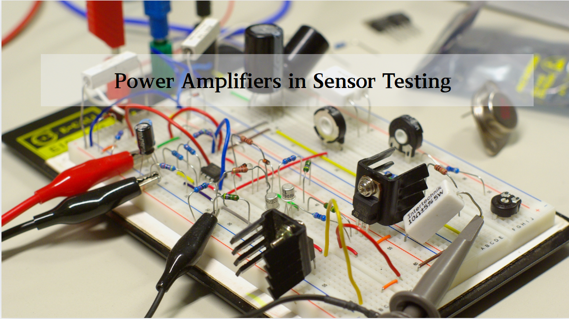
Multivariate Application Analysis of Power Amplifiers in Sensor Testing
In the field of modern sensor testing, power amplifiers (PAs) serve as core components and play an indispensable role. From amplifying weak signals to simulating complex physical environments, power amplifiers provide solid guarantees for the precise testing of sensor performance through their uniqu...
-
2025 / 06 / 28
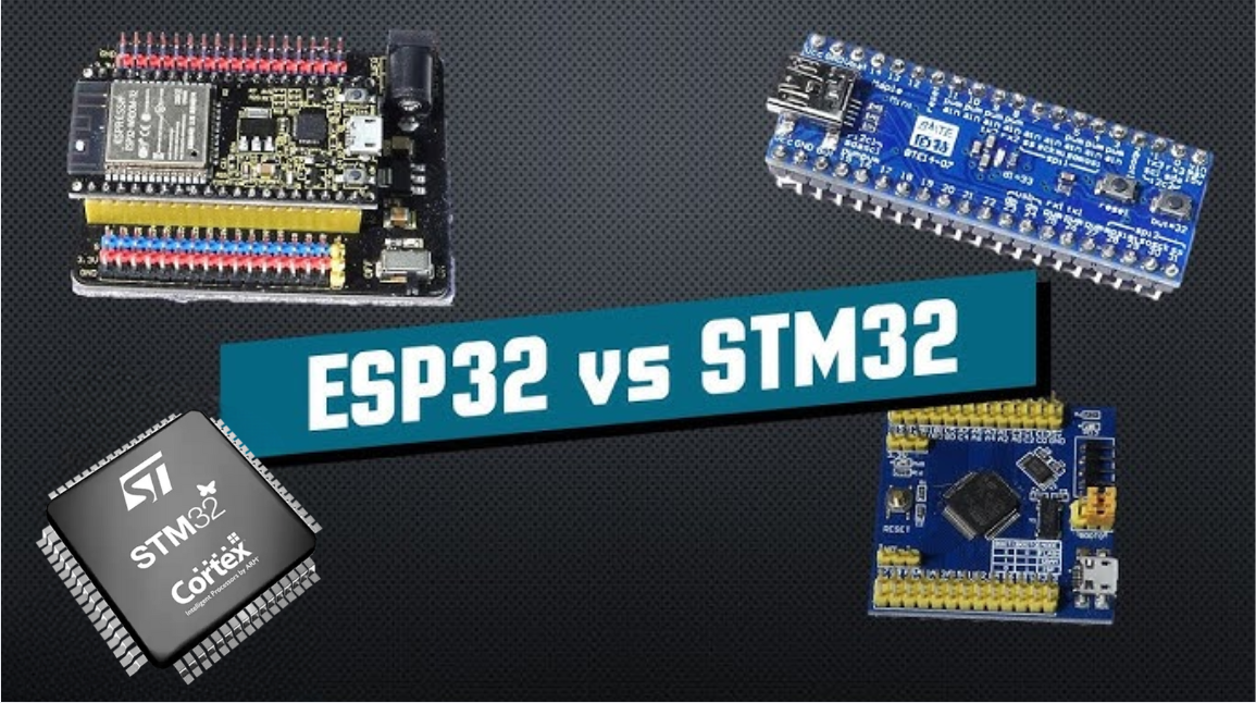
ESP32 vs STM32: Which Microcontroller Suits You Better?
In the field of embedded development, both ESP32 and STM32 are highly favored microcontrollers, each with unique features and advantages. When facing project development, how do you choose between them? This requires comprehensive consideration of multiple factors. The following detailed comparison ...
-
2025 / 06 / 26
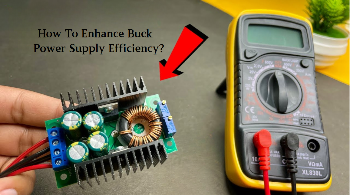
Key Strategies to Enhance Buck Power Supply Efficiency
Improving the efficiency of Buck (step-down) switching power supplies requires a multi-dimensional approach targeting energy loss sources, including component selection, topology optimization, control strategies, and thermal management. Below are core strategies and engineering practices:...
-
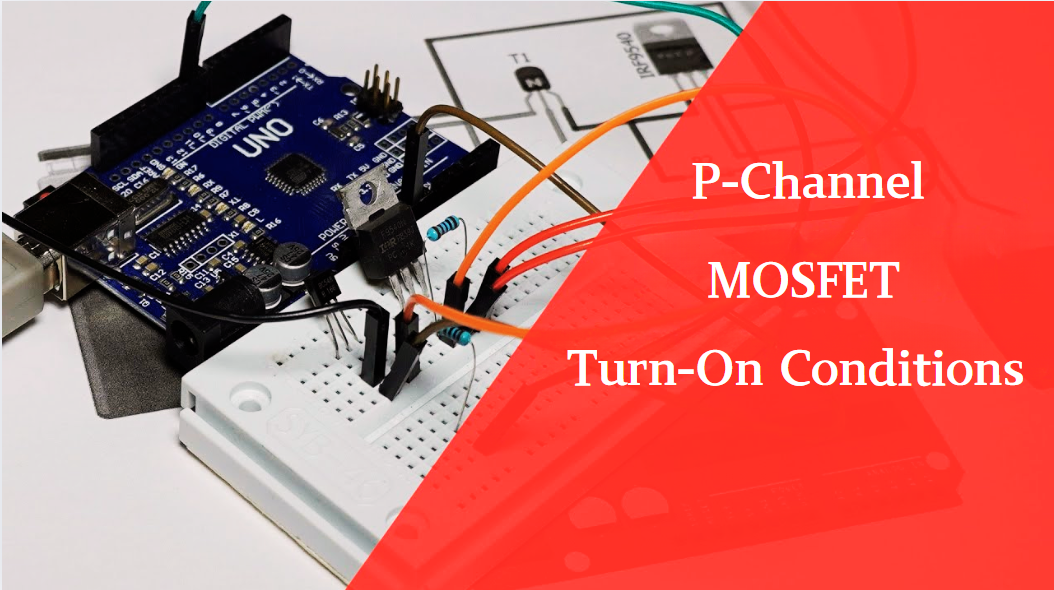
2025 / 06 / 26
P-Channel MOSFET Turn-On Conditions
The turn-on conditions for a P-channel MOSFET (PMOS) are inverse to those of an N-channel MOSFET (NMOS), primarily governed by the relationship between the gate-source voltage (VGS) and the threshold voltage (Vth), along with voltage polarity. Here are the key points:A PMOS turns on when its gate vo...
-
2025 / 06 / 24
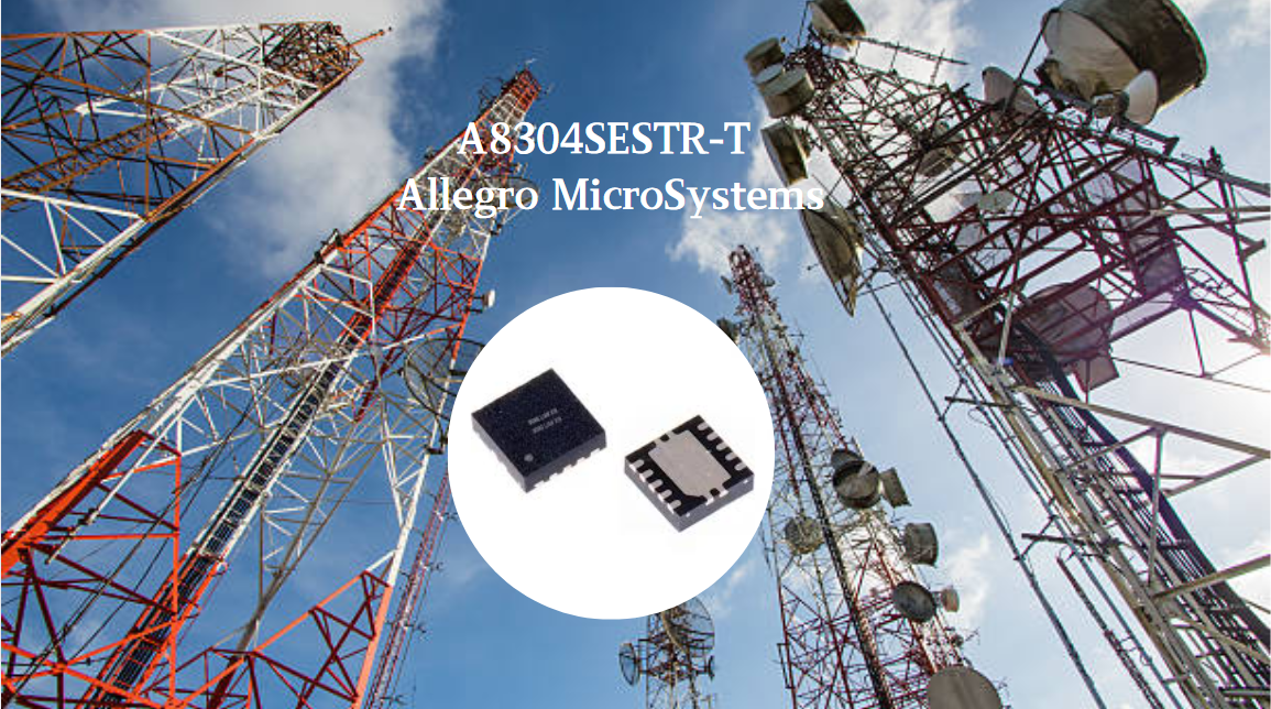
A8304SESTR-T Allegro MicroSystems-Single LNB Supply and Control Voltage Regulator
The Allegro MicroSystems A8304SESTR-T is a single-channel Low Noise Block Regulator (LNBR). It integrates a monolithic boost converter with MOSFET, current sensing, and compensation. Featuring a 704 kHz switching frequency, it uses few external components. With an I²C-compatible interface, it offers...
-
2025 / 06 / 20
EG25GGC-128-SGNS by Quectel Wireless Solutions Co., Ltd: Features,Symbol,Footprint and Datasheet
The Quectel EG25GGC - 128 - SGNS is an LTE Cat 4 module optimized for M2M and IoT. Supporting 3GPP Rel. 11, it offers up to 150Mbps downlink and 50Mbps uplink. With global LTE/UMTS/GSM coverage, it's backward - compatible with EDGE/GPRS. Featuring multi - constellation GNSS (GPS, GLONASS, BeiDou, et...


2000+
Daily average RFQ Volume

30,000,000
Standard Product Unit

2800+
Worldwide Manufacturers

15,000 m2
In-stock Warehouse
 Wishlist (0 Items)