

- RFQ
- BOM
-
Contact Us
Tel: +86-0755-83501315
Email: sales@sic-components.com


- Chinese
- English
- French
- German
- Portuguese
- Spanish
- Russian
- Japanese
- Korean
- Arabic
- Irish
- Greek
- Turkish
- Italian
- Danish
- Romanian
- Indonesian
- Czech
- Afrikaans
- Swedish
- Polish
- Basque
- Catalan
- Esperanto
- Hindi
- Lao
- Albanian
- Amharic
- Armenian
- Azerbaijani
- Belarusian
- Bengali
- Bosnian
- Bulgarian
- Cebuano
- Chichewa
- Corsican
- Croatian
- Dutch
- Estonian
- Filipino
- Finnish
- Frisian
- Galician
- Georgian
- Gujarati
- Haitian
- Hausa
- Hawaiian
- Hebrew
- Hmong
- Hungarian
- Icelandic
- Igbo
- Javanese
- Kannada
- Kazakh
- Khmer
- Kurdish
- Kyrgyz
- Latin
- Latvian
- Lithuanian
- Luxembou..
- Macedonian
- Malagasy
- Malay
- Malayalam
- Maltese
- Maori
- Marathi
- Mongolian
- Burmese
- Nepali
- Norwegian
- Pashto
- Persian
- Punjabi
- Serbian
- Sesotho
- Sinhala
- Slovak
- Slovenian
- Somali
- Samoan
- Scots Gaelic
- Shona
- Sindhi
- Sundanese
- Swahili
- Tajik
- Tamil
- Telugu
- Thai
- Ukrainian
- Urdu
- Uzbek
- Vietnamese
- Welsh
- Xhosa
- Yiddish
- Yoruba
- Zulu
- Kinyarwanda
- Tatar
- Oriya
- Turkmen
- Uyghur
Comprehensive Comparison Analysis of Analog and Digital Switch ICs
I. Core Definitions and Essential Differences
1. Analog Switch ICs https://www.sic-components.com/switches
Analog switches are solid-state electronic switches based on complementary MOSFETs (parallel P-channel and N-channel), capable of bidirectional signal transmission for both analog signals (e.g., audio, video, sensor voltages) and digital signals. Their core characteristics include:
Voltage Compatibility: Supports a wide range of signals from low voltage (3.3V) to high voltage (±600V, such as Littelfuse CPC7560);
Cutoff Isolation Mechanism: Achieves >10⁹Ω high-impedance isolation through SOI process or oxide layers, with typical isolation reaching -110dB@5kHz (required for medical ultrasound scenarios);
Bidirectional Conduction Design: Channel formation is controlled by gate voltage, with on-resistance as low as 1Ω (TI TS5A3166) and high-voltage types around 12.5Ω (Monolithic MP4816).
2. Digital Switch ICs
Digital switches only process TTL/CMOS logic levels (0/1), with the output mirroring the input logic state. The essential differences from analog switches lie in:
Signal Limitation: Inability to transmit continuous analog quantities, only supporting digital signal routing (e.g., SPI/I2C buses, GPIO expansion);
Cutoff State Characteristics: Returns to high-impedance state (Hi-Z, such as TI SN74CB3Q3253) or fixed level (74HC4066), with isolation impedance around 10⁶Ω and risk of leakage current;
Simplified Structure: Mostly uses single N-channel MOSFETs, requiring only 3.3V/5V TTL levels for logic control, making the drive circuit simpler.
II. Working Principles and Structural Comparison
Characteristics Analog Switch ICs Digital Switch ICs
Signal Type Analog signals (±90V ultrasonic pulses/audio waveforms) + digital signals Only digital signals (3.3V/5V logic levels, USB data)
Conduction Mechanism P+N channel complementary conduction, supporting bidirectional current transmission (ABLIC ±100V) N-channel unidirectional conduction, logic level mirroring (NXP 74HC4051)
Cutoff Isolation 10⁹Ω high impedance (SOI process), blocking signal coupling 10⁶Ω low impedance, potential crosstalk (isolation -60dB@1kHz)
Control Signal Digital logic/analog voltage (5V drives ±100V switches) Strictly matches TTL/CMOS (3.3V/5V levels non-interchangeable)
Typical Applications High-voltage path control, audio switching, sensor signal acquisition Bus expansion, digital signal gating, power on/off control
III. Key Performance Parameter Differences
1. Core Parameters of Analog Switch ICs
(1) On-Resistance RDS(on)
Definition: Total resistance between source and drain when conducting, directly affecting signal attenuation (P=I²×R) and distortion.
Typical Values:
Low-voltage audio: 1Ω (TI TS5A3166, THD+N<0.001%);
High-voltage medical: 12.5Ω (Monolithic MP4816, ±90V ultrasonic probe);
Industrial high-voltage: 50Ω (Littelfuse ±600V devices).
Impact: Every 10Ω increase in RDS(on) adds 0.1W of power consumption at 100mA current, exacerbating phase distortion at high frequencies.
(2) Off Isolation
Quantification Index: Expressed in decibels, e.g., Littelfuse CPC7560 reaches -110dB@5kHz, meaning crosstalk signal amplitude <0.01%.
Critical Scenarios: In medical ultrasound equipment, insufficient isolation (e.g., <80dB) causes probe signal crosstalk, resulting in B-scan image ghosting.
(3) Frequency Response and Parasitic Capacitance
Limiting Factors: Channel parasitic capacitance (CISS=50pF/COSS=15pF) causes high-frequency attenuation, with typical bandwidth <100MHz.
Engineering Case: Maxim MAX4617 has 1dB insertion loss at 10MHz, requiring a 100Ω/100MHz bead + 100nF capacitor for compensation.
(4) Switching Speed (tON/tOFF)
Audio Applications: <1ms to avoid audible pops (TI DRV2605L switching time 500μs);
High-Voltage Scenarios: 100ns level (Littelfuse ±320V devices), suitable for fast switching of 20MHz ultrasonic pulses.
2. Core Parameters of Digital Switch ICs
(1) Logic Level Compatibility
Matching Principles:
3.3V CMOS systems: Choose 74LVC series (e.g., SN74LVC1G08, input threshold 1.35V);
5V TTL systems: Choose 74HC series (e.g., NXP 74HC4051, input threshold 2V).
(2) Maximum Data Transmission Rate
Bottleneck Parameters:
Conduction delay tPD=5ns (ADI ADG1608), determining the maximum clock frequency;
Rise/fall time tr/tf=2ns, supporting 100Mbps USB 2.0 signals (NRZ encoding).
(3) Default State Design
High-Impedance State (Hi-Z): Such as TI SN74CB3Q3253, which outputs high impedance when off to avoid multi-device bus contention (e.g., I2C bus conflicts);
Fixed Level: 74HC4066 outputs a default high level when OE# is low, simplifying MCU initialization logic.
IV. Comparative Analysis of Application Scenarios
1. Typical Applications of Analog Switch ICs
(1) Medical Ultrasound Imaging Systems
Pain Points: Transmitting ±90V high-voltage pulses to excite piezoelectric crystals while ensuring crosstalk between 16 channels < -80dB.
Solution: Monolithic MP4816 (16-channel SPST, RDS(on)=12.5Ω), powered by a single +180V supply, saving 40% volume compared to traditional positive/negative supply schemes. Integrated output bleed resistors avoid probe aftershock interference, improving image resolution by 15%.
(2) Industrial High-Voltage Testing Equipment
Technical Challenges: ±300V test voltage, 20MHz sine wave, requiring switch loss <0.5W.
Scheme Design: Littelfuse CPC7532 (±320V, 14.5Ω) with a π-type impedance matching network (100Ω+10nF). 100ns switching speed enables distortion-free transmission of 20MHz signals, with isolation >100dB during multi-channel parallel testing and testing accuracy reaching ±0.1%.
(3) New Energy Vehicle Battery Management
Core Requirements: 400V battery pack charge/discharge control, standby current <1μA, high-frequency switching (100kHz).
Technical Breakthrough: Power Integrations InnoMux™-2 (1700V GaN switch), RDS(on)=8mΩ, reducing conduction loss by 70% compared to silicon devices. Supports 100kHz high-frequency switching, reducing on-board charger volume by 50% and efficiency up to 90%.
2. Typical Applications of Digital Switch ICs
(1) High-Speed Bus Expansion and Level Conversion
Application Scenario: Extending the MCU's SPI bus from 3.3V to 5V, supporting 10Mbps data rate.
Optimal Solution: TI SN74AVC16245 (16-bit bidirectional converter), with built-in tri-state outputs and Schmitt trigger inputs, transmission delay <10ns, and 5V tolerant inputs to avoid level conflicts in 3.3V/5V system interconnection.
(2) Automotive Electronics Power Management
Scenario Requirements: Controlling camera power in a 12V vehicle system, switching delay <100ns, requiring over-temperature protection.
Component Selection: Infineon BTS5040 (intelligent high-side switch), integrating over-temperature shutdown (150°C threshold), short-circuit protection, and diagnostic functions, with quiescent current <5μA, supporting PWM dimming (200Hz~10kHz).
(3) Automated Test Equipment (ATE)
Functional Requirements: Multi-channel digital signal gating (e.g., 64-channel GPIO expansion), supporting 50MHz clock signals, bit error rate <10⁻⁹.
Scheme Configuration: Maxim MAX306 (8-channel SPST) used in cascade, paired with a clock buffer (e.g., TI CDCLV1108), switching delay 5ns, rise time 2ns, meeting the high-speed testing needs of ATE equipment.
V. Selection Decision Guide
1. Signal Type Priority Principle
Analog Signal-Dominant Scenarios: Must use analog switches (e.g., sensor voltage acquisition, audio mixing, high-voltage pulse transmission);
Pure Digital Signal Scenarios: Prioritize digital switches (e.g., MCU IO expansion, logic level conversion, bus routing), with costs reduced by 30%~50%.
2. Key Parameter Evaluation Process
(1) Four-Step Analog Switch Selection
Voltage Margin Calculation: Working voltage ×1.5 ≤ device voltage resistance (e.g., select ±320V devices for 220V industrial systems, ×2 margin for automotive cold start scenarios);
RDS(on) Power Budget: Calculated based on maximum operating current: RDS(on)<10Ω at 100mA (power <0.1W), <1Ω at 1A;
Isolation Scenario Matching: >50dB@1MHz for high-frequency RF switching, >110dB@5kHz for medical ultrasound;
Switching Timing Verification: Medical equipment requires Break-Before-Make (BBM) characteristics (tON>tOFF) to avoid signal short-circuiting; industrial control can use Make-Before-Break (MBB) characteristics (tON<tOFF) to prevent open circuits.
(2) Three Key Elements of Digital Switch Selection
Logic Level Matching: Choose 74LVC/74AVC series for 3.3V systems, 74HC/HCT series for 5V systems, noting input thresholds and output drive capabilities (e.g., sink/source current);
Data Rate Calculation: Based on signal rise time tr=0.35/BW, ensure switch bandwidth > signal maximum frequency (e.g., 10MHz square wave requires BW>35MHz);
Default State Design: Bus applications must select high-impedance state (Hi-Z); power control scenarios prefer OE# low-level effective (default cutoff) to avoid power-on misoperation.
VI. Technical Development Trends
1. Innovation Directions for Analog Switches
Wide Bandgap Material Breakthroughs: SiC MOSFETs for 1200V high-voltage analog switches (RDS(on)<5mΩ), suitable for photovoltaic inverters and energy storage systems, reducing switching losses by 80%;
System-Level Integration: ADI ADG1609 integrates ±15kV ESD protection, latch protection, and diagnostic functions, reducing peripheral components by 50%, applicable to industrial automation scenarios.
2. Technological Evolution of Digital Switches
High-Speed Interface Adaptation: TI SN65LV1023 supports 3.125Gbps PCIe 2.0 signal switching, delay <10ns, meeting high-speed bus expansion for servers;
Intelligence and Automotive Grade: Infineon BTS5040 adds open-circuit detection and overcurrent protection, certified by AEC-Q100, improving reliability in automotive electronics by 30%, with fault diagnosis response time <10μs.
VII. Conclusion
Analog and digital switch ICs play irreplaceable differentiated roles in electronic systems: the former, as a "high-voltage bridge" for analog signals, must balance voltage resistance, on-resistance, and signal isolation, suitable for medical ultrasound, industrial high-voltage, and other scenarios; the latter, as a "high-speed router" for digital logic, focuses on level compatibility, data transmission rate, and integration, leading in bus expansion, power control, and other fields. With the popularization of third-generation semiconductor materials (SiC/GaN) and 3D integration processes, analog switches are breaking through the 1200V voltage resistance bottleneck and developing toward low resistance, while digital switches are moving toward intelligence through Gbps-level transmission and built-in diagnostic functions. In practical selection, engineers should take signal type as the core, combine voltage level, power budget, and scenario reliability requirements, accurately match device parameters, and promote the continuous evolution of signal chain systems in medical, automotive, new energy, and other fields toward high integration, low power consumption, and intelligence.
https://www.sic-components.com/switches
Hot Products
View More-

R7A-CRZ010C Omron Automation and Safety
-
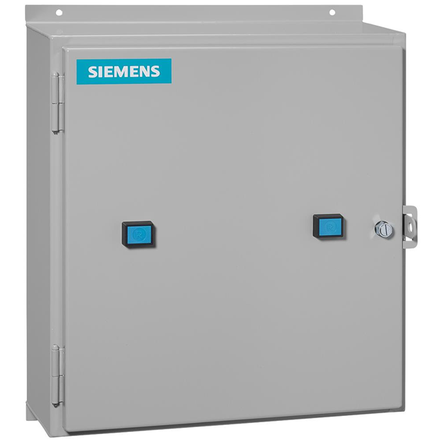
22EUE32AJ Siemens
-
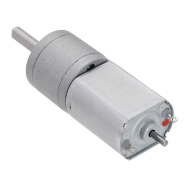
3470 Pololu Corporation
-
3RA21201DQ270AK6 Siemens
-
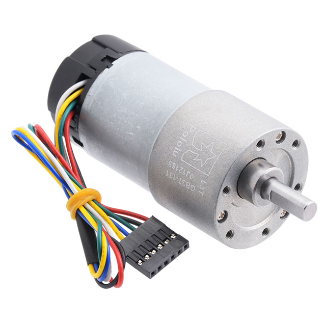
4756 Pololu Corporation
-
US2:83FUF95EH Siemens
-
6SL32303YH180UF0 Siemens
-
EAMC-30-32-10-10 Festo Corporation
-
EMMB-AS-60-02-S30SB Festo Corporation
-
3RA21150CD151BB4 Siemens
-
3RE41224BA311KH3 Siemens
-
EASC-G1-45-100 Festo Corporation
Related Blogs
-
2025 / 07 / 09
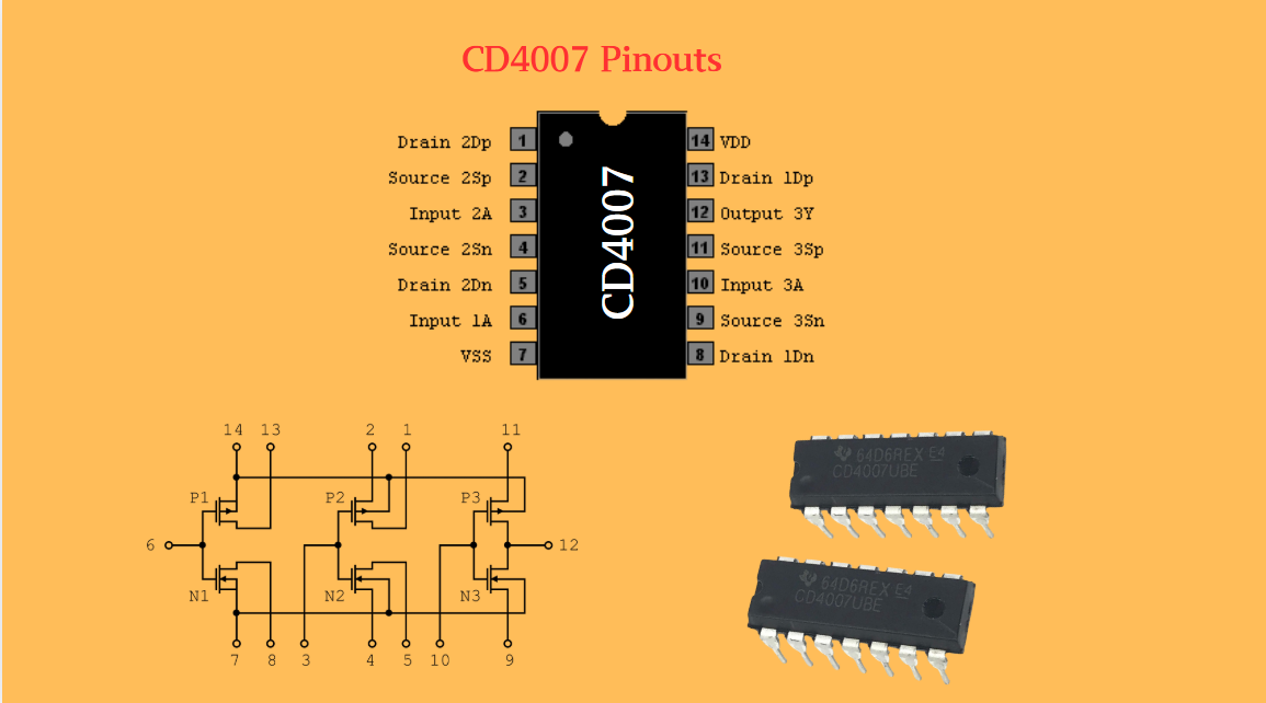
CD4007: A Comprehensive Analysis of a Multifunctional CMOS Integrated Circuit
In the field of modern electronic technology, CMOS (Complementary Metal-Oxide-Semiconductor) integrated circuits have become core components in digital and analog circuit design due to their low power consumption, high integration, and excellent compatibility. As a classic CMOS device, the CD4007 oc...
-
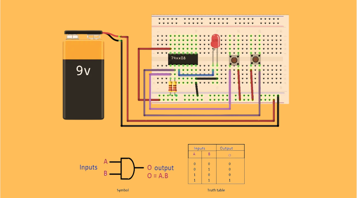
2025 / 07 / 07
Understanding IC 7408: A Fundamental Component in Digital Logic Design
In the vast and intricate realm of digital electronics, integrated circuits (ICs) serve as the building blocks that enable the creation of complex and powerful systems. Among these, the IC 7408 holds a special place as a fundamental component in digital logic design. This article aims to provide a c...
-
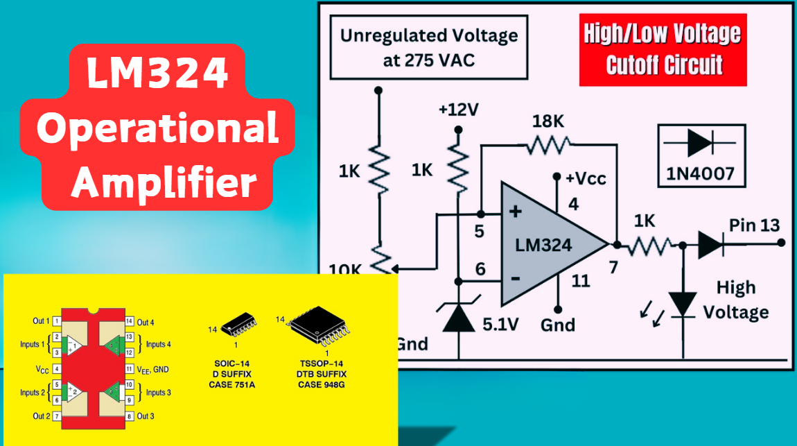
2025 / 07 / 04
LM324 Operational Amplifier Comprehensive Guide: Pins, Applications, Packaging, and Datasheet
The LM324 is a low-cost integrated circuit featuring four independent operational amplifiers (op-amps), renowned for its wide voltage adaptability, low power consumption, and high reliability in industrial and consumer electronics. With a single-supply voltage range of 3V to 32V (or dual-supply rang...
-
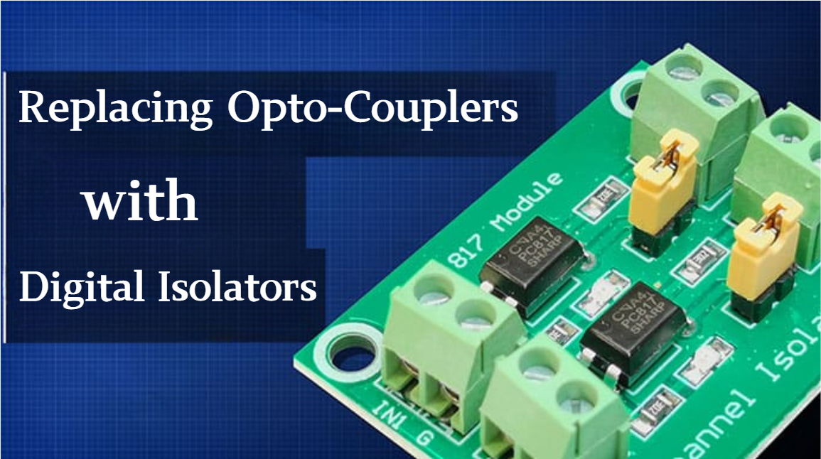
2025 / 07 / 02
A Comprehensive Guide to Replacing Opto-Couplers with Digital Isolators: From Principles to Practice
In the ever-evolving landscape of electronic design, the transition from opto-couplers to digital isolators marks a pivotal shift in isolation technology. For decades, opto-couplers have been the cornerstone of electrical isolation in industrial control, medical devices, and power systems, relying o...
-
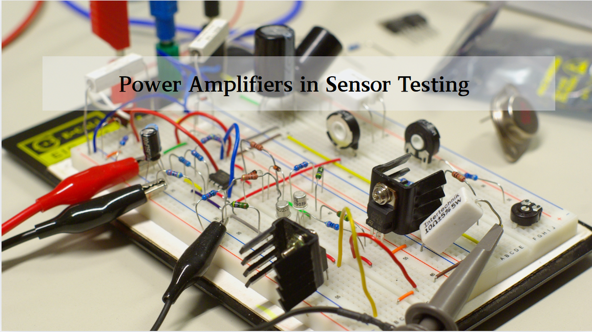
2025 / 06 / 30
Multivariate Application Analysis of Power Amplifiers in Sensor Testing
In the field of modern sensor testing, power amplifiers (PAs) serve as core components and play an indispensable role. From amplifying weak signals to simulating complex physical environments, power amplifiers provide solid guarantees for the precise testing of sensor performance through their uniqu...
-
2025 / 06 / 28
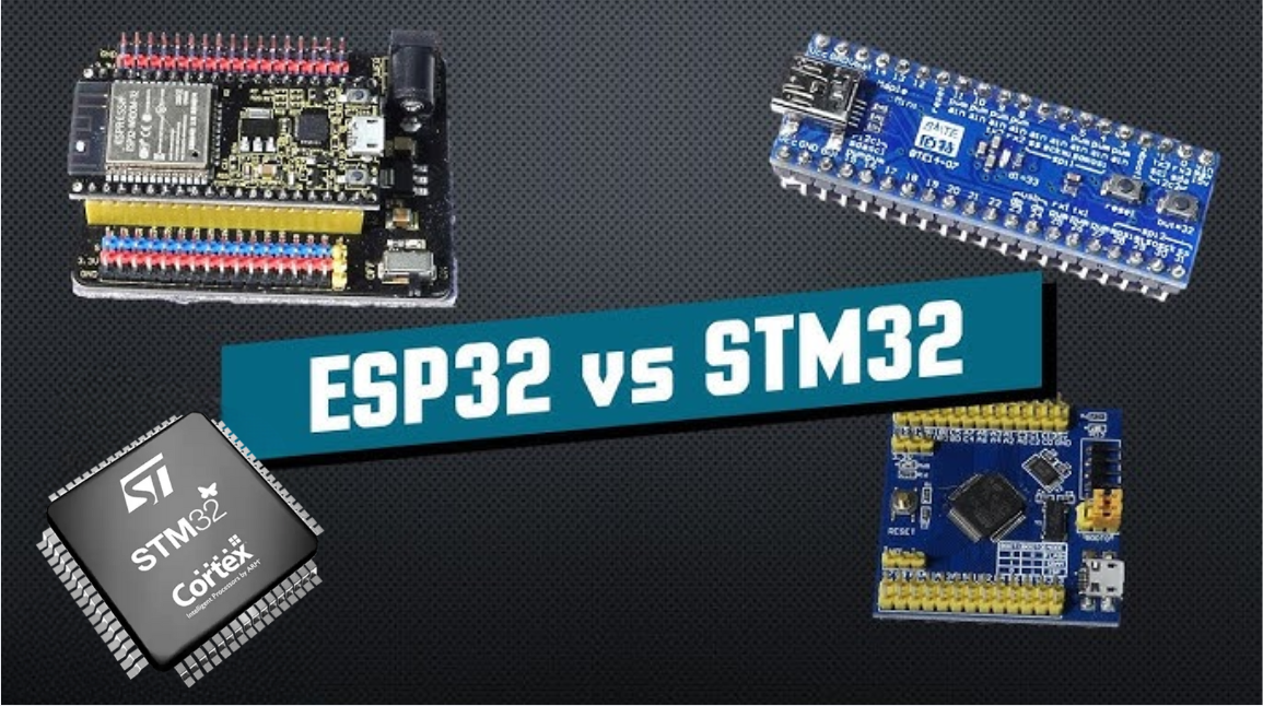
ESP32 vs STM32: Which Microcontroller Suits You Better?
In the field of embedded development, both ESP32 and STM32 are highly favored microcontrollers, each with unique features and advantages. When facing project development, how do you choose between them? This requires comprehensive consideration of multiple factors. The following detailed comparison ...
-
2025 / 06 / 26
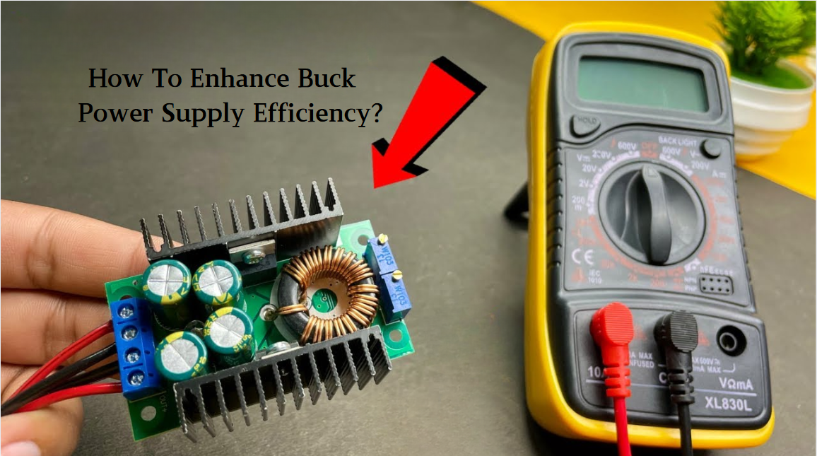
Key Strategies to Enhance Buck Power Supply Efficiency
Improving the efficiency of Buck (step-down) switching power supplies requires a multi-dimensional approach targeting energy loss sources, including component selection, topology optimization, control strategies, and thermal management. Below are core strategies and engineering practices:...
-
2025 / 06 / 26
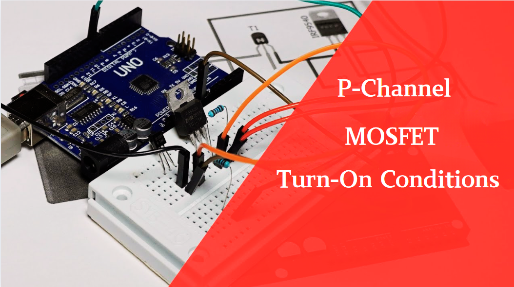
P-Channel MOSFET Turn-On Conditions
The turn-on conditions for a P-channel MOSFET (PMOS) are inverse to those of an N-channel MOSFET (NMOS), primarily governed by the relationship between the gate-source voltage (VGS) and the threshold voltage (Vth), along with voltage polarity. Here are the key points:A PMOS turns on when its gate vo...
-
2025 / 06 / 24
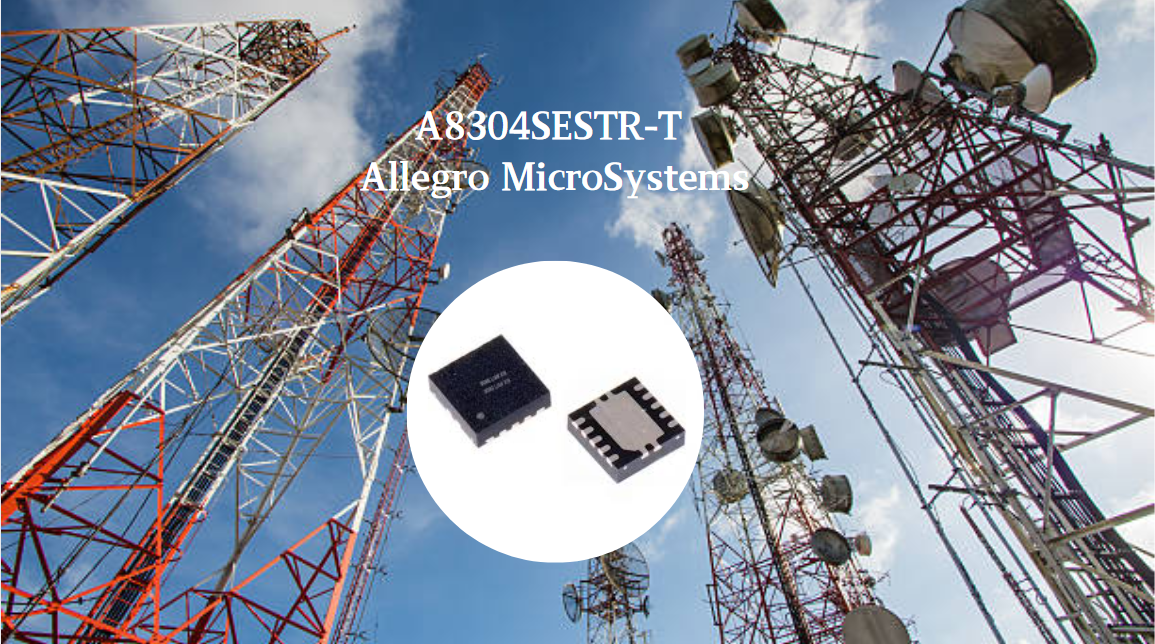
A8304SESTR-T Allegro MicroSystems-Single LNB Supply and Control Voltage Regulator
The Allegro MicroSystems A8304SESTR-T is a single-channel Low Noise Block Regulator (LNBR). It integrates a monolithic boost converter with MOSFET, current sensing, and compensation. Featuring a 704 kHz switching frequency, it uses few external components. With an I²C-compatible interface, it offers...
-
2025 / 06 / 20
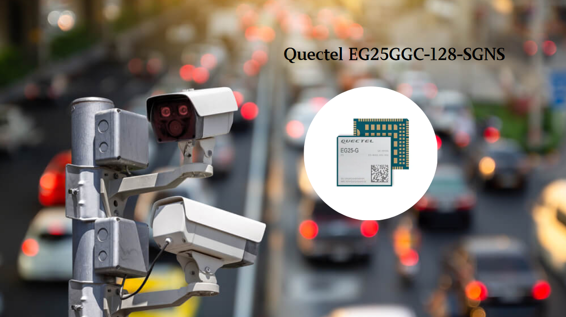
EG25GGC-128-SGNS by Quectel Wireless Solutions Co., Ltd: Features,Symbol,Footprint and Datasheet
The Quectel EG25GGC - 128 - SGNS is an LTE Cat 4 module optimized for M2M and IoT. Supporting 3GPP Rel. 11, it offers up to 150Mbps downlink and 50Mbps uplink. With global LTE/UMTS/GSM coverage, it's backward - compatible with EDGE/GPRS. Featuring multi - constellation GNSS (GPS, GLONASS, BeiDou, et...

2000+
Daily average RFQ Volume

30,000,000
Standard Product Unit

2800+
Worldwide Manufacturers

15,000 m2
In-stock Warehouse
 Wishlist (0 Items)