In the vast landscape of semiconductor devices, MOSFETs (Metal - Oxide - Semiconductor Field - Effect Transistors) play a pivotal role, especially in power electronics. Among the numerous MOSFET models available, the P55NF06 stands out for its unique combination of features, making it suitable for a wide range of applications. This article delves deep into the world of P55NF06 MOSFET, exploring its technical specifications, working principles, applications, and advantages over other similar devices.
What is A P55NF06 N-Channel Power MOSFET?
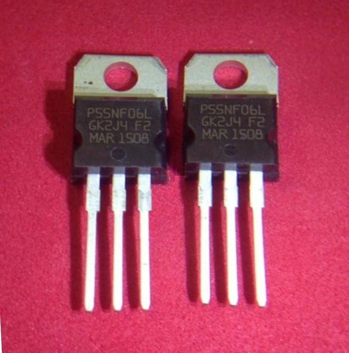
The P55NF06 is an N - channel power MOSFET launched by STMicroelectronics. It has a rated voltage of 60V and a continuous drain current of 50A at 25°C. With an ultra - low on - resistance (typical value of 0.018Ω), it can significantly reduce power consumption. It features fast switching speed and excellent dynamic performance, suitable for high - current and high - speed switching applications such as motor control, DC - DC converters. Packaged in TO - 220, it has good heat dissipation performance. It is widely used in automotive electronics, like fuel injection systems, ABS, and airbag systems, due to its high reliability.
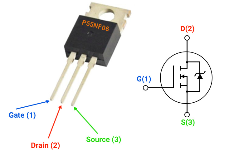
P55NF06 MOSFET Pinout Configuration

| Pin Number | Pin Name | Description |
|---|---|---|
| 1 | G | Gate - This pin is used to control the flow of current between the source and drain. By applying a voltage to the gate, the MOSFET can be turned on or off. |
| 2 | D | Drain - This pin is connected to the load or circuit that you want to switch or control using the MOSFET. When the MOSFET is turned on, current can flow from the source to the drain. |
| 3 | S | Source - This pin is connected to the ground or negative terminal of the power supply. When the MOSFET is turned on, current can flow from the source to the drain. |
P55NF06 MOSFET Technical Specifications
| Parameter | Content |
|---|---|
| Model | STP55NF06 |
| Package | TO-220 FP-3 |
| Lot Number | 19+ |
| Manufacturer | STMicroelectronics |
| Product Type | MOSFET |
| RoHS | Yes |
| Mounting Style | Through Hole |
| Number of Channels | 1 Channel |
| Transistor Polarity | N-Channel |
| Vds - Drain-Source Breakdown Voltage | 60 V |
| Id - Continuous Maximum Drain Current at Tc = 25 °C | 50 A |
| Rds On - Drain-Source On-State Resistance | 15 mOhms |
| Vgs - Gate-Source Voltage | 20 V |
| VGS(th) - Gate-Source Threshold Voltage Vds | 3 V |
| Idm - Pulsed Drain Current | 200 A |
| Qg - Total Gate Charge | 44.5 nC |
| Minimum Operating Junction Temperature | -55 C |
| Maximum Operating Junction Temperature | +175 C |
| Pd - Power Dissipation | 30 W |
| Configuration | Single |
| Channel Mode | Enhancement |
| Height | 9.3 mm |
| Length | 10.4 mm |
| Series | STP55NF06FP |
| Transistor Type | 1 N-Channel |
| Width | 4.6 mm |
| Forward Transconductance - Min | 18 S |
| Fall Time | 15 ns |
| Rise Time | 50 ns |
| Typical Turn-Off Delay Time | 36 ns |
| Typical Turn-On Delay Time | 20 ns |
| Unit Weight | 2.040 g |
Key Features of P55NF06 MOSFET
The P55NF06 N-Channel Power MOSFET, produced by STMicroelectronics, is engineered for high-performance applications. Here are its key features:
Low On-Resistance (RDS(on))
Extremely low typical RDS(on) of 18 mΩ (at VGS = 10V), minimizing conduction losses and heat generation.
Enables efficient power handling in high-current applications.
High Current Capability
Continuous drain current (ID) of 50A (at 25°C), suitable for motor control, DC-DC converters, and power supplies.
Can handle peak currents up to 200A, making it robust for transient loads.
Voltage Rating
Drain-source voltage (VDS) rating of 60V, providing a safety margin for applications with voltage spikes.
Fast Switching Speed
Low gate charge (Qg ~ 72 nC) and short rise/fall times, enabling rapid switching in PWM circuits.
Ideal for high-frequency applications (e.g., switching regulators up to 100kHz+).
Thermal Performance
TO-220 package with excellent thermal conductivity, allowing efficient heat dissipation.
Power dissipation (PD) of 150W (with proper heatsinking).
Enhanced Ruggedness
Avalanche energy rated (EAS) for reliable operation under inductive loads.
Built-in protection against overcurrent and overvoltage conditions.
Logic-Level Compatible
Gate threshold voltage (VGS(th)) of ~2-4V, compatible with standard logic outputs (e.g., 5V microcontrollers).
P55NF06 Equivalent MOSFETs
For high-current applications, there are various MOSFETs that can replace the P55NF06. Notable equivalent models include the 110N10, 65N06, 50N06, 75N06, and 80N06. These models offer comparable voltage and current handling capabilities, making them suitable for intensive power management tasks. For instance, when a slightly lower current capacity is acceptable, the 50N06 and 65N06 models are ideal choices, as they can optimize power consumption and reduce heat output, thereby extending system lifespan and improving efficiency.
For applications requiring different voltage thresholds or with packaging constraints, models such as the BR75N75, BR80N75, and BUK7509-75A are ideal. These MOSFETs balance power handling capability and physical size, providing design flexibility without compromising performance. They are well-suited for applications that demand specific operating characteristics (e.g., different voltage handling capacities or better thermal management) which the P55NF06 may not offer.
For applications operating under extremely high frequencies or harsh thermal conditions, alternative products from International Rectifier, such as the IRF1405, IRF2807, IRF3205, IRF3256, and IRF4410A, can be considered. These MOSFETs are renowned for their reliability in harsh environments like automotive applications. The IRF3205 and IRF3256 are specifically designed to withstand the rigorous operating conditions of high-stress applications.
For designs requiring fine-tuning of switching speed, resistance values, or gate charge characteristics, MOSFETs such as the IRFB3207, IRFB4710, IRFB7740, and IRFZ44N offer a range of options. These models allow designers to precisely match the MOSFET to their specific needs.
Principles of P55NF06 MOSFET
The P55NF06, an N - channel MOSFET, has three terminals: gate (G), source (S), and drain (D). A positive voltage on the gate relative to the source generates an electric field. This field pulls electrons from the source, forming an N - type channel between source and drain. When gate - source voltage (VGS) surpasses the ~3V threshold, channel conductivity jumps, letting drain - to - source current (ID) flow. If VGS stays below that threshold, the MOSFET stays off, barely any current passing between drain and source.

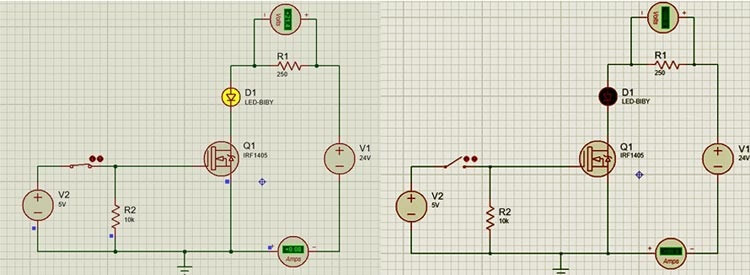
P55NF06 MOSFET Simulated Circuit
In the on - state, its drain - source on - resistance (RDS(on)) is really low, around 0.018Ω. That low resistance makes current conduction efficient, cutting down power lost as heat. Like, in the given circuit, when the right VGS hits Q1 (the IRF1405, which works similarly), current can flow through the LED to light it up.
Also, it has relatively low input capacitance (Ciss) and gate charge (Qg). These help it switch fast. Low Ciss lets the gate - source capacitance charge and discharge quickly, making the on - off transitions rapid—super important for stuff like DC - DC converters that need high - speed switching. It’s neat how these little aspects all work together to make the MOSFET do its job, y’know?
Pros And Cons Of P55NF06 MOSFET
The P55NF06 N-channel power MOSFET offers a balance of performance and versatility for medium-voltage, high-current applications, but it also has limitations. Here are its key pros and cons:
Pros
High Current Handling: With a continuous drain current (ID) of 50A (at 25°C) and peak current up to 200A, it reliably supports high-load applications like motor drives and power converters.
Low Conduction Losses: Its ultra-low on-resistance (RDS(on) ≈ 18 mΩ at VGS=10V) minimizes energy loss during conduction, improving overall system efficiency.
Moderate Voltage Rating: A 60V drain-source voltage (VDS) provides a safe margin for applications with voltage spikes, suitable for 12V/24V systems (e.g., automotive, industrial).
Fast Switching: Low gate charge (≈72 nC) and quick rise/fall times enable efficient operation in high-frequency PWM circuits, such as DC-DC converters.
Robust Thermal Performance: The TO-220 package offers excellent heat dissipation, supporting up to 150W power dissipation with proper heatsinking, critical for high-current scenarios.
Avalanche Ruggedness: Rated for avalanche energy (EAS), it withstands inductive load transients, enhancing reliability in motor control and inverter applications.
Cost-Effective: Balances performance and affordability, making it a budget-friendly choice for industrial and automotive auxiliary systems.
Cons
Limited Voltage Range: The 60V VDS rating restricts use in high-voltage applications (e.g., 48V+ systems), where higher-voltage MOSFETs (e.g., 100V+) are needed.
Not Logic-Level Optimized: While functional with 10V gate drive, its gate threshold (VGS(th) = 2–4V) may require additional gate drivers for reliable operation with 3.3V logic, unlike true logic-level MOSFETs.
Package Constraints: The TO-220 package, though thermally efficient, is bulkier than surface-mount alternatives (e.g., D2PAK), limiting use in space-constrained designs.
Higher Gate Charge Than Some Alternatives: Compared to newer MOSFETs, its gate charge (72 nC) is moderate, which may slightly reduce switching efficiency in ultra-high-frequency (e.g., >200kHz) applications.
Sensitivity to Overvoltage Spikes: Beyond 60V, it lacks protection, requiring external clamping circuits in environments prone to large voltage transients (e.g., heavy industrial machinery).
P55NF06 MOSFET Applications
The P55NF06, an N-channel power MOSFET with a 60V voltage rating and 50A continuous current capability, is widely used in various high-current, medium-voltage applications due to its low on-resistance, fast switching speed, and robust performance. Its key application scenarios include:
Motor Control Systems: Ideal for driving DC motors, brushless DC motors (BLDC), and stepper motors in industrial equipment, robotics, and automotive auxiliary systems. Its high current handling capacity ensures stable operation even under load fluctuations.
Power Supplies and Converters: Used in DC-DC buck/boost converters, voltage regulators, and switched-mode power supplies (SMPS) for consumer electronics, industrial machinery, and battery-powered devices. It efficiently handles power conversion with minimal energy loss.
Automotive Electronics: Applied in automotive subsystems such as electric power steering, lighting controls, and battery management systems (BMS). Its rugged design withstands the harsh electrical and thermal environments of vehicles.
Inverters and Power Inverters: Suitable for small-scale inverters that convert DC power (from batteries or solar panels) to AC, powering household appliances or portable equipment.
Battery Charging Systems: Integrated into battery chargers for electric tools, EV auxiliary batteries, and energy storage systems, managing charging currents and ensuring safe operation.
Load Switches and Protection Circuits: Functions as a high-current load switch in power distribution circuits, with fast switching enabling quick response to overcurrent or short-circuit conditions, protecting downstream components.
Industrial Automation: Used in programmable logic controllers (PLCs), motor drives, and sensor modules, providing reliable power switching in factory automation setups.
Comparative Analysis with Other MOSFETs
The P55NF06 MOSFET has its own set of pros and cons when it comes to parameters and performance. When you stack it up against other MOSFETs, things get interesting. Take low-current ones like the 2N7002, for example—those are mostly for small-signal switching, topping out at a few hundred milliamps. The P55NF06, though, can handle 50A continuously, which is a huge leap. That makes it way better for high-current jobs like motor control or beefy DC-DC converters.
Then there are high-voltage MOSFETs such as the IRF840, which can take 500V. The P55NF06 maxes out at 60V, so it’s out of its depth in high-voltage setups. But in 12V or 24V systems? It shines. Its on-resistance is way lower than those high-voltage types, which is a big plus when you’re dealing with low voltage and high current.
Logic-level MOSFETs like the IRLZ44N are a different story. They’re built to work with low gate voltages, around 5V, which is super convenient for microcontrollers. The P55NF06 can be driven by a microcontroller too, but it really needs around 10V to turn on fully. That’s a bit of a hassle compared to the IRLZ44N, honestly.
High-frequency specialists, like the SiC MOSFET C2M0080120D, are in a league of their own. They’ve got tiny switching losses and can run at hundreds of kilohertz or more. The P55NF06 switches fast enough, but its gate charge is on the higher side. It’s fine for general high-frequency stuff, like up to 100kHz, but in ultra-high-frequency scenarios? Not so much.
Even among similar-rated MOSFETs—50N06, 65N06—the P55NF06 holds its own. The 50N06 matches its 50A current, but the P55NF06 has lower on-resistance, which means less power wasted. The 65N06 can handle 65A, but its on-resistance is a bit higher. So overall, the P55NF06 is more efficient in those cases.
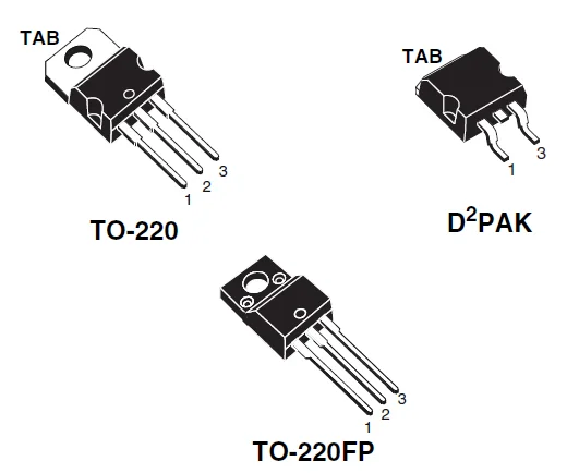
STP55NF06 packages

The STP55NF06 MOSFET is available in several package types. The most common one is the TO-220 package. This package is easy to install and has good heat - dissipation performance, which is beneficial for the STP55NF06 to work stably in high - current applications6. In addition, it may also be packaged in D²PAK and TO-220FP formats. The D²PAK package can provide a more compact layout in some cases, which is suitable for applications with limited space. The TO-220FP package may also have its own characteristics in heat - dissipation and installation, but the specific performance needs to be determined according to the actual product design.
Hot-selling products of SIC
71421LA55J8 UPD44165184BF5-E40-EQ3-A SST39VF800A-70-4C-B3KE IS66WV1M16DBLL-55BLI-TR AS4C32M16SB-7BIN W25Q16FWSNIG
AS7C34098A-20JIN 752369-581-C W957D6HBCX7I TR IS61LPS12836EC-200B3LI MX25L12875FMI-10G QG82915PL
Product information is from SIC Electronics Limited. If you are interested in the product or need product parameters, you can contact us online at any time or send us an email: sales@sic-chip.com.
Frequently Asked Questions [FAQ]
1. What is the maximum drain-source voltage (Vds) of the P55NF06 MOSFET?
The maximum drain-source voltage (Vds) of the P55NF06 MOSFET is 60 volts. This is the absolute limit for the voltage that can safely be applied between the drain and source terminals. Go above 60V, and the device is likely to fail immediately—so you’ve got to nail this in circuit design.
2. How does temperature affect the performance of the P55NF06 MOSFET?
When temperatures rise, this MOSFET starts to underperform. Its on-resistance increases, leading to higher power dissipation, and its current-carrying capacity takes a hit. Running it hot long-term isn’t just bad for performance—it’s like a slow death for the device, drastically shortening its lifespan. So, getting the heat management right is non-negotiable.
3. What precautions should be taken when handling and installing the P55NF06 MOSFET?
Antistatic measures are a must when handling and installing this part. Use an ESD wristband or antistatic mat—static electricity can fry it in an instant, which is a total waste. Also, don’t bend the leads too hard, and watch the soldering temperature—physical or thermal damage is easy to avoid if you’re careful.
4. Can the P55NF06 MOSFET be directly driven by a microcontroller?
Technically, yes—if the microcontroller’s output voltage covers the MOSFET’s gate threshold (typically 2–4V). But for high-frequency or high-current apps, a gate driver is way better. Without it, the microcontroller might struggle to drive the MOSFET efficiently, slowing down switching and hurting performance. Kinda defeats the purpose, right?
5. How does the P55NF06 MOSFET handle inductive loads?
It can handle inductive loads (like motors or transformers), but there’s a catch: switching inductive loads creates voltage spikes that can blow the MOSFET. The fix? Add a freewheeling diode to clamp those spikes. Skip this, and you’re asking for a fried device—it’s that simple.
6. What is the input capacitance (Ciss) of the P55NF06 MOSFET?
Its typical input capacitance (Ciss) is around 1350 pF. This matters a lot for high-frequency switching—higher capacitance slows down gate charging/discharging, dragging down switching speed. So, the driver circuit needs to account for this to keep things snappy.
7. How to choose the right heatsink for the P55NF06 MOSFET?
Start by calculating the actual power dissipation of the device. Then, pick a heatsink that can handle that heat, keeping the MOSFET within its safe operating temperature range. Skimping on the heatsink here is a rookie move—overheating will just cause constant issues.
8. What protection circuits are recommended for the P55NF06 MOSFET?
Overvoltage, overcurrent, and overtemperature protection are basics. Also, high-speed switching can create voltage spikes, so adding a snubber circuit (like an RC or RCD network) helps suppress those. Skip these, and the MOSFET might fail unexpectedly—total hassle.
9. How to test the functionality of the P55NF06 MOSFET before use?
A multimeter works for a quick check: the gate-source should read open, and the drain-source should also be open with no gate voltage. Apply enough gate voltage, and the drain-source should conduct with low resistance. For peace of mind, a quick load test in a simple circuit to check switching behavior is smart—better safe than sorry.
10. What are common failure modes of the P55NF06 MOSFET?
Common ways it fails: thermal overload (bad heatsinking), gate oxide breakdown (from excessive gate-source voltage), or voltage spikes exceeding its ratings. These failures are usually permanent, so preventing them with good design is way easier than replacing parts.


 Wishlist (0 Items)