

- RFQ
- BOM
-
Contact Us
Tel: +86-0755-83501315
Email: sales@sic-components.com


- Chinese
- English
- French
- German
- Portuguese
- Spanish
- Russian
- Japanese
- Korean
- Arabic
- Irish
- Greek
- Turkish
- Italian
- Danish
- Romanian
- Indonesian
- Czech
- Afrikaans
- Swedish
- Polish
- Basque
- Catalan
- Esperanto
- Hindi
- Lao
- Albanian
- Amharic
- Armenian
- Azerbaijani
- Belarusian
- Bengali
- Bosnian
- Bulgarian
- Cebuano
- Chichewa
- Corsican
- Croatian
- Dutch
- Estonian
- Filipino
- Finnish
- Frisian
- Galician
- Georgian
- Gujarati
- Haitian
- Hausa
- Hawaiian
- Hebrew
- Hmong
- Hungarian
- Icelandic
- Igbo
- Javanese
- Kannada
- Kazakh
- Khmer
- Kurdish
- Kyrgyz
- Latin
- Latvian
- Lithuanian
- Luxembou..
- Macedonian
- Malagasy
- Malay
- Malayalam
- Maltese
- Maori
- Marathi
- Mongolian
- Burmese
- Nepali
- Norwegian
- Pashto
- Persian
- Punjabi
- Serbian
- Sesotho
- Sinhala
- Slovak
- Slovenian
- Somali
- Samoan
- Scots Gaelic
- Shona
- Sindhi
- Sundanese
- Swahili
- Tajik
- Tamil
- Telugu
- Thai
- Ukrainian
- Urdu
- Uzbek
- Vietnamese
- Welsh
- Xhosa
- Yiddish
- Yoruba
- Zulu
- Kinyarwanda
- Tatar
- Oriya
- Turkmen
- Uyghur
INA128: A Comprehensive Guide to the Precision Instrumentation Amplifier
The INA128, a product of Texas Instruments (TI), stands as a premier example of a precision instrumentation amplifier. Engineered for applications demanding high accuracy and stability, it combines low offset voltage, low drift, and high common - mode rejection ratio (CMRR). This article delves into the INA128's architecture, key specifications, application scenarios, and practical design considerations.
1. Architecture and Core Principles
1.1 Three - Op - Amp TopologyT
he INA128 employs the classic three - operational - amplifier (three - op - amp) configuration, a design celebrated for its exceptional common - mode rejection and differential gain capabilities. This setup consists of two input - stage op - amps and one output - stage op - amp.Input Stage: The two input op - amps are tasked with buffering the differential inputs. They also set the amplifier's gain through an external resistor RG. This stage is crucial for rejecting common - mode signals, such as noise that appears identically on both input terminals.Output Stage: The third op - amp takes the amplified differential signal from the input stage and converts it into a single - ended output. It ensures that the output signal is referenced to a stable ground or another appropriate reference voltage.
1.2 Gain Configuration
A defining feature of the INA128 is its flexible gain - setting mechanism. The gain G of the amplifier can be precisely adjusted using an external resistor RG according to the formula G = 1+50KΩ/Rg. This allows users to tailor the gain to their specific application requirements, whether it's amplifying very small signals, such as those from sensors, or processing signals of moderate amplitude.
2. Key Specifications
2.1 Electrical Performance
Low Offset Voltage: The INA128 exhibits a maximum input offset voltage of 500 μV. This low offset voltage is critical in applications where small signals need to be accurately amplified, as it minimizes errors introduced by the amplifier itself.
Low Drift: With a maximum offset voltage drift of 2 μV/°C, the INA128 maintains its accuracy over a wide temperature range. This is particularly important in environments where temperature variations are significant, such as industrial and automotive applications.
High CMRR: The common - mode rejection ratio of the INA128 is typically 100 dB at a gain of 100. This high CMRR enables the amplifier to effectively suppress common - mode noise, making it ideal for applications where the signal of interest is accompanied by significant common - mode interference.
Bandwidth: The INA128 has a gain - bandwidth product of 100 kHz. This bandwidth is suitable for a wide range of applications, including sensor signal conditioning and low - frequency data acquisition.
2.2 Power and Thermal Characteristics
Low Power Consumption: Operating on a dual power supply ranging from ±2.25 V to ±18 V, the INA128 consumes a quiescent current of only 2.2 mA. This low power consumption makes it suitable for battery - powered applications and other systems where power efficiency is a concern.
Wide Temperature Range: The INA128 is designed to operate reliably over a temperature range of −40°C to +85°C. This wide temperature range allows it to be used in harsh environments, such as industrial and automotive settings.
3. Applications
3.1 Sensor Signal Conditioning
Sensors, such as strain gauges, thermocouples, and pressure sensors, often produce very small signals that are susceptible to noise. The INA128 is well - suited for amplifying these weak sensor signals while rejecting common - mode noise. For example, in a strain - gauge - based load cell, the INA128 can amplify the small voltage changes generated by the strain gauge, providing a signal that is large enough for further processing by an analog - to - digital converter (ADC).
3.2 Data Acquisition Systems
In data acquisition systems, the INA128 plays a vital role in preparing analog signals for digital conversion. It ensures that the signals are amplified to an appropriate level and that common - mode noise is minimized. This results in more accurate digital representation of the analog signals, which is essential for applications such as scientific measurements and industrial process control.
3.3 Medical Instrumentation
Medical devices, such as electrocardiogram (ECG) machines and blood pressure monitors, require high - precision amplification of bioelectric signals. The INA128's low offset voltage, low drift, and high CMRR make it an excellent choice for these applications. It can accurately amplify the weak electrical signals generated by the body while rejecting external interference, such as power - line noise.
3.4 Industrial Process Control
In industrial process control systems, the INA128 is used to amplify and condition signals from various sensors, such as temperature sensors and flow meters. It helps in maintaining the accuracy and reliability of the control system by providing clean, amplified signals that can be used to make informed control decisions.
4. Practical Design Considerations4.1 External ComponentsGain Resistor RG: The choice of the external gain resistor RG is critical as it directly determines the gain of the INA128. To achieve precise gain, it is advisable to use a high - precision resistor with a low temperature coefficient. This ensures that the gain remains stable over time and across different temperature conditions.Filtering Capacitors: Adding bypass capacitors between the power supply pins and ground is essential to reduce power - supply noise. These capacitors help in maintaining a clean power supply for the amplifier, which is crucial for its optimal performance.
4.2 PCB Layout
Signal Routing: Proper signal routing on the printed circuit board (PCB) is necessary to minimize noise and interference. The input signals should be routed away from high - current or high - frequency traces to avoid coupling of unwanted signals.
Grounding: A well - designed grounding scheme is vital for the INA128. A star - grounding technique, where all ground connections meet at a single point, can help in reducing ground loops and minimizing noise.
4.3 Power Supply Decoupling
To ensure stable operation, the INA128 requires proper power - supply decoupling. This involves placing bypass capacitors close to the power - supply pins of the amplifier. The capacitors should be chosen based on their capacitance value and frequency response to effectively filter out both high - frequency and low - frequency noise from the power supply.
5. Comparison with Similar Amplifiers
When compared to other instrumentation amplifiers on the market, the INA128 stands out for its combination of low cost, good precision, and wide availability. While there are other amplifiers with even lower offset voltage or higher CMRR, they often come at a higher cost. The INA128 provides a good balance between performance and cost, making it a popular choice for a wide range of applications.
6. Conclusion
The INA128 is a versatile and reliable instrumentation amplifier that offers high precision, low power consumption, and excellent common - mode rejection. Its flexible gain configuration and robust performance make it suitable for a variety of applications, from sensor signal conditioning to medical instrumentation. By understanding its architecture, key specifications, and practical design considerations, engineers can effectively utilize the INA128 to design high - quality analog circuits that meet the requirements of their specific applications. Whether in industrial, medical, or data - acquisition systems, the INA128 continues to be a trusted component for precision signal amplification.
https://www.ti.com/lit/ds/symlink/ina128.pdf


Hot Products
View More

Related Blogs
-
2025 / 08 / 29
Top 10 Electronic component Manufacturing Companies in China
China's electronic component industry is reshaping the global supply chain landscape at a 12% annual compound growth rate (CAGR). According to 2023 data from the China Electronic Components Industry Association, domestic enterprises hold over 35% of the global market share in segments such as connec...

-
2025 / 08 / 20
Altera FLEX 10K Embedded Programmable Logic Device Family: A Milestone in Programmable System Integr
As the industry's first embedded programmable logic device (PLD) family launched by Altera (now part of Intel Programmable Solutions Group), the FLEX 10K series redefined the role of programmable logic devices in system-level integration with its innovative "embedded array + logic array" architectur...

-
2025 / 08 / 19
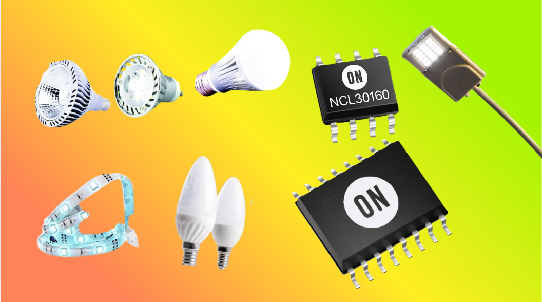
LED Driver IC: A Comprehensive Overview
An LED driver IC is an integrated circuit specifically designed to regulate the power supplied to light-emitting diodes (LEDs), ensuring they operate within safe and optimal electrical parameters. Unlike traditional light sources, LEDs are current-dependent devices, making precise current and voltag...
-
2025 / 08 / 18
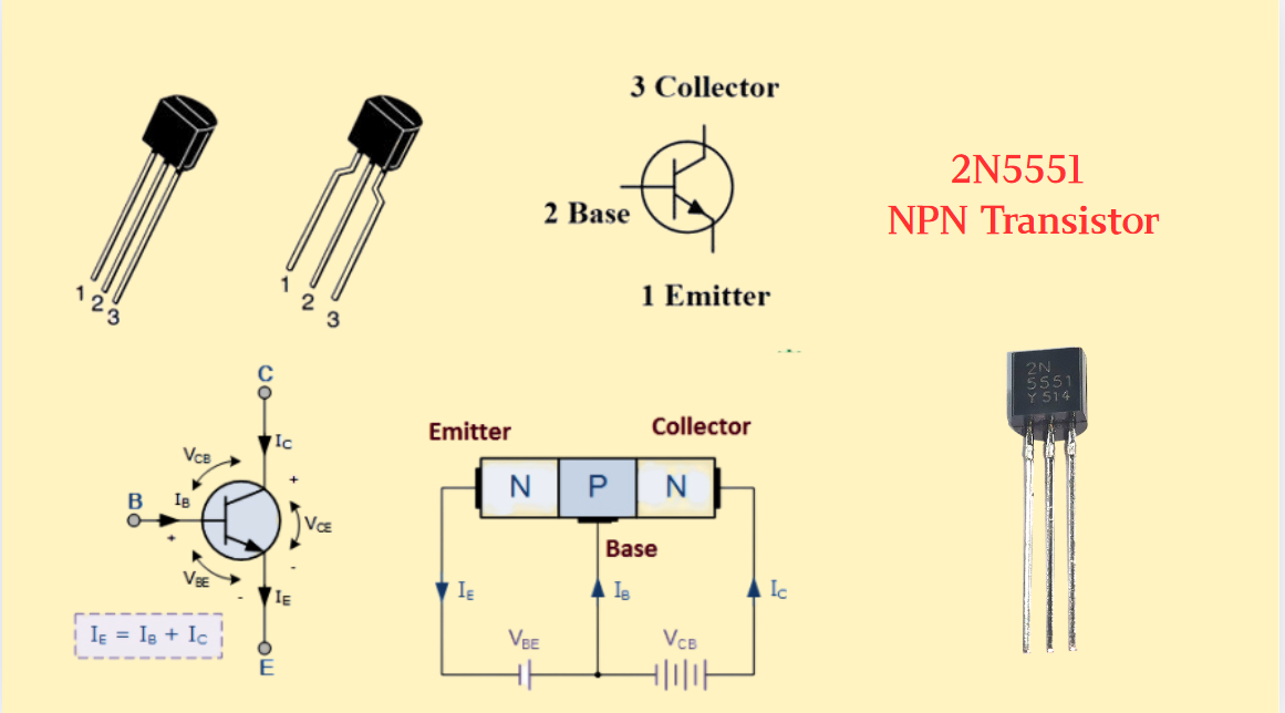
2N5551 NPN Transistor:Features,Applications,Datasheet and Pinout
In the vast realm of electronics, transistors serve as the unsung heroes, powering countless devices and circuits that have become an integral part of our daily lives. Among them, the 2N5551 NPN transistor stands out as a versatile and widely - utilized component. With its unique combination of feat...
-
2025 / 08 / 14
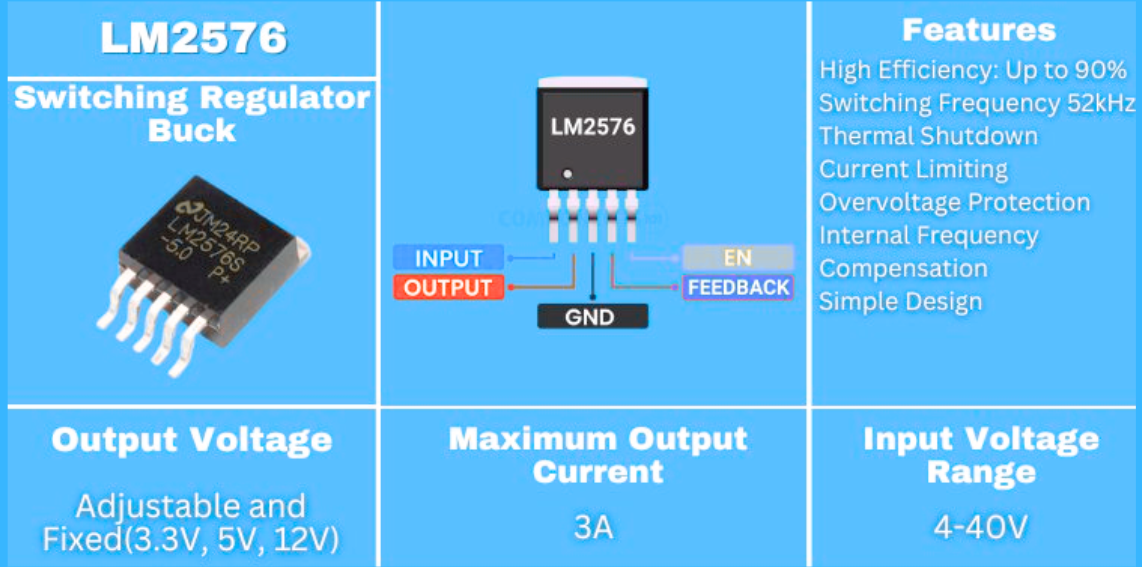
Step-Down Voltage Regulator LM2576 In-Depth Analysis: A Comprehensive Guide from Features to Applica
LM2576 is a classic step-down switching regulator introduced by Texas Instruments (TI). Since its launch, it has occupied an important position in the field of DC power conversion. With its mature technology, stable performance, and wide applicability, it has become a benchmark product in medium and...
-
2025 / 08 / 12
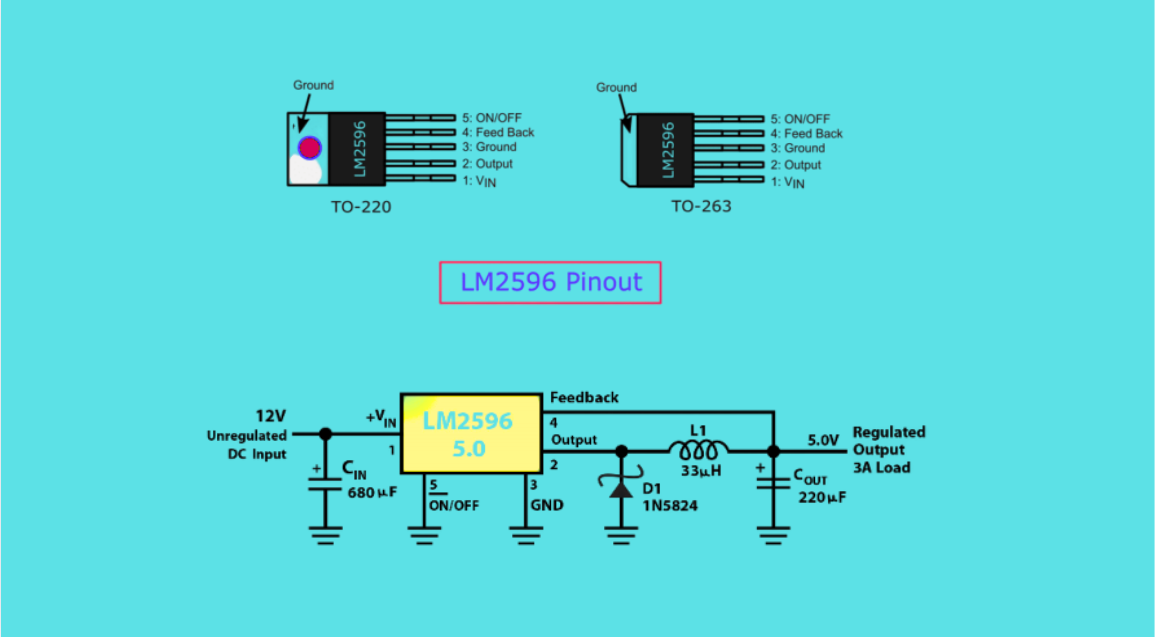
LM2596 Voltage Regulator: Replacements, Performance Traits, Internal Architecture and Practical Uses
The LM2596 series voltage regulators are monolithic integrated circuits that provide all active functions for step-down (buck) switching regulators. They can drive 3A loads with excellent line and load regulation capabilities. This series of devices includes versions with fixed output voltages of 3....
-
2025 / 08 / 07
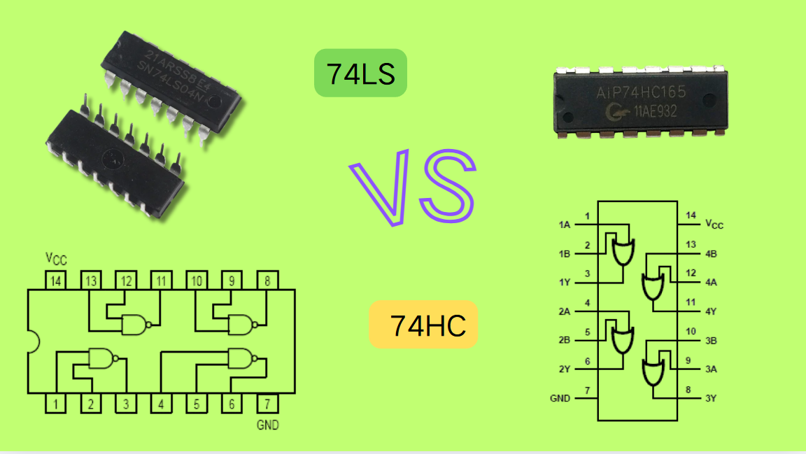
74HC vs 74LS Series ICs: A Comprehensive Comparison
The 74 series of integrated circuits (ICs) has been the backbone of digital electronics for decades, enabling the design of logic gates, flip-flops, counters, and other essential digital building blocks. Among the most popular variants are the 74HC and 74LS series, each optimized for specific applic...
-
2025 / 08 / 06
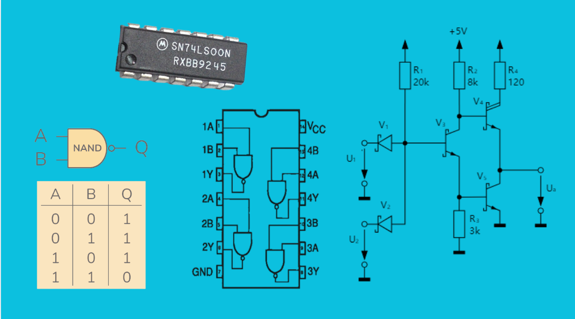
74LS00: Functions, Applications,Features and Datasheet
The 74LS00 is a widely used TTL (Transistor-Transistor Logic) integrated circuit that functions as a quad 2-input NAND gate. This means it contains four independent NAND gates, each with two input pins and one output pin. Each NAND gate in the 74LS00 performs the "NAND" logical operation: the output...
-
2025 / 08 / 01
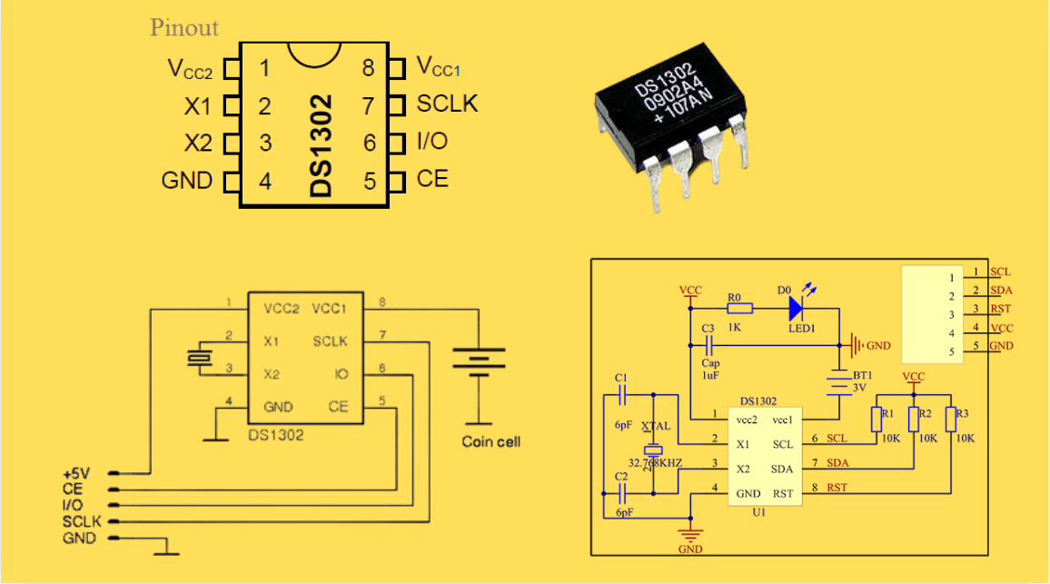
DS1302 RTC: Datasheet,Attributes,Features,Applications
As a low-power device widely used in electronic equipment, the DS1302 is centered on accurate real-time clock/calendar recording functions. It supports full-dimensional tracking of seconds, minutes, hours, days, weeks, months, and years, features automatic leap year compensation, and is compatible w...
-
2025 / 07 / 30
LT3097 Dual 500 mA, positive/negative, ultralow noise, ultrahigh PSRR low dropout linear regulator
The LT3097 is a dual, positive and negative, high-performance, low-dropout linear regulator featuring Analog Devices, Inc., ultralow noise and ultra-high power supply rejection ratio (PSRR) architecture for powering noise-sensitive applications. Each regulator delivers up to 500 mA with a typical 26...


2000+
Daily average RFQ Volume

30,000,000
Standard Product Unit

2800+
Worldwide Manufacturers

15,000 m2
In-stock Warehouse
 Wishlist (0 Items)