

- RFQ
- BOM
-
Contact Us
Tel: +86-0755-83501315
Email: sales@sic-components.com


- Chinese
- English
- French
- German
- Portuguese
- Spanish
- Russian
- Japanese
- Korean
- Arabic
- Irish
- Greek
- Turkish
- Italian
- Danish
- Romanian
- Indonesian
- Czech
- Afrikaans
- Swedish
- Polish
- Basque
- Catalan
- Esperanto
- Hindi
- Lao
- Albanian
- Amharic
- Armenian
- Azerbaijani
- Belarusian
- Bengali
- Bosnian
- Bulgarian
- Cebuano
- Chichewa
- Corsican
- Croatian
- Dutch
- Estonian
- Filipino
- Finnish
- Frisian
- Galician
- Georgian
- Gujarati
- Haitian
- Hausa
- Hawaiian
- Hebrew
- Hmong
- Hungarian
- Icelandic
- Igbo
- Javanese
- Kannada
- Kazakh
- Khmer
- Kurdish
- Kyrgyz
- Latin
- Latvian
- Lithuanian
- Luxembou..
- Macedonian
- Malagasy
- Malay
- Malayalam
- Maltese
- Maori
- Marathi
- Mongolian
- Burmese
- Nepali
- Norwegian
- Pashto
- Persian
- Punjabi
- Serbian
- Sesotho
- Sinhala
- Slovak
- Slovenian
- Somali
- Samoan
- Scots Gaelic
- Shona
- Sindhi
- Sundanese
- Swahili
- Tajik
- Tamil
- Telugu
- Thai
- Ukrainian
- Urdu
- Uzbek
- Vietnamese
- Welsh
- Xhosa
- Yiddish
- Yoruba
- Zulu
- Kinyarwanda
- Tatar
- Oriya
- Turkmen
- Uyghur
Switch ICs: Comprehensive Guide to Power Control and Intelligent Protection
I. Essential Definition and Technical Positioning of Switch ICs https://www.sic-components.com/switches
Switch integrated circuits (Switch ICs) are a category of integrated power management chips that achieve precise control over power on/off states and circuit protection through built-in semiconductor switching devices (such as MOSFETs, IGBTs) and protection circuits. Compared with traditional mechanical switches, their core advantages include:
Semiconductor-level switching performance: Leveraging MOSFET on/off characteristics, switching speed reaches the nanosecond level (typical delay <50ns), supporting high-frequency PWM control above 100kHz.
Fully integrated protection functions: Built-in overcurrent (OCP), overvoltage (OVP), and over-temperature (OTP) protection modules, with response time <10μs (e.g., TI TPS2595 shuts down within 15μs under 10A overload).
Low power consumption and small size: Standby leakage current <1μA, using miniature packages like SOT-23 and WSON (size 1.5x1.5mm), saving 60% PCB space compared to discrete solutions.
Technical architecture: Composed of three parts: logic control unit, power switch unit, and protection monitoring unit. Typical on-resistance as low as 10mΩ (60V voltage rating), supporting current control from microamps to 10 amperes.
II. Classification System and Typical Application Scenarios
1. Classification by Function and Application
(1) USB Switches: Power Gatekeepers for Consumer Electronics
Core features: Support USB PD 3.1 (28V voltage rating), integrated EMI filtering and hot-swap protection.
Typical model: TI TPS2596 (10A continuous current, foldback current limiting design).
Application cases: USB-C interface power switching for laptops (e.g., Dell XPS series), fast charging protocol adaptation for smartphones.
(2) Rectifier Switches: Polarity-Insensitive Power Adaptation
Technical advantages: Automatically identify input polarity, support dry battery reverse connection protection (e.g., ROHM BD7492FJ).
Performance indicators: Forward voltage drop <0.3V@1A, 15% higher efficiency than traditional Schottky diodes.
Application scenarios: Children's toys (compatible with reverse battery installation), power management for medical handheld devices (glucometers).
(3) Load Switches: Terminators of Standby Power Consumption
Energy-saving mechanism: Impedance >10^9Ω when off (e.g., ADI ADG1608), integrated soft start to suppress inrush current.
Key parameters: On-resistance 1.2Ω@5V, switching delay <100ns.
Typical scenarios: Secondary power switching for smartphones (camera power control), sleep mode power management for digital cameras (standby power <50μW).
(4) Intelligent Power Switches (IPS): Industrial-Grade Protection Hubs
Intelligent features: Support I2C/SPI communication, real-time feedback of temperature/current (e.g., Infineon OptiMOS™ 5 series).
Safety standards: Fault diagnosis accuracy reaches single-channel level, compliant with ISO 26262 ASIL-B.
Industrial applications: PLC power distribution, MPPT module switching for photovoltaic inverters.
(5) Battery Line Switches: Power Hubs for Mobile Devices
Technical highlights: Support lithium battery overcharge protection, integrated power monitoring (e.g., TI BQ24295).
Performance indicators: 4.5V-28V wide input voltage, charging efficiency >95%.
Application scenarios: Battery charge/discharge management for laptops, power path control for tablet PCs.
III. Key Technical Parameters and Selection Criteria
1. Electrical Parameters Priority Matrix
Parameter Category Key Indicator Selection Recommendation
Voltage Rating (Vds) ≥1.5× operating voltage USB applications select >20V (e.g., Vishay 30V models)
Continuous Current (Iout) Capacity after 20% derating at 85℃ Server applications select >10A (e.g., TI LP5907)
On-Resistance (Rds(on)) <50mΩ@12V (automotive grade) Preferred <10mΩ (GaN solutions)
Switching Delay <100ns (high-frequency scenarios) PWM control select <50ns (e.g., EPC2055)
Standby Leakage Current <1μA (IoT devices) Industrial grade can relax to 10μA
2. Packaging and Thermal Design Considerations
Low thermal resistance packaging: DFN-8L package thermal resistance Rth(j-a)=40℃/W, 50% lower than SOT-23.
PCB layout principles:
Power path copper cladding ≥2mm², thermal vias ≥4.
Parallel 100nF ceramic capacitors at input/output to suppress ripple.
3. Typical Selection Cases
Application Scenario Recommended Model Core Parameters Advantage Highlights
USB PD Fast Charging PI INN257 650V voltage rating, 1.5A continuous current Integrated X-capacitor discharge function
Automotive BCM NXP TJA1010 -40℃~125℃ wide temperature, 50mΩ on-resistance AEC-Q100 certified, EMI-resistant design
Photovoltaic Inverter Silicon Labs Si74605 80V voltage rating, 10A switching current Support 100kHz PWM
IV. In-Depth Analysis of Working Principles and Protection Mechanisms
1. Electrical Process of Switching Action
On Stage:
Logic input (EN/IN) applies high level (≥2V).
Gate driver circuit charges, MOSFET channel turns on, current Id=Vds/Rds(on).
Off Stage:
Logic input low level, gate charge 泄放 through discharge resistor (10kΩ~100kΩ).
Channel pinches off, leakage current <1nA (ideal state).
2. Protection Function Implementation Mechanisms
Overcurrent Limiting (OCP):
Current sampled via sense resistor, comparator triggers logic shutdown, typical foldback current limiting (e.g., 3A overload reduced to 1A).
Over-Temperature Protection (OTP):
Thermistor monitors junction temperature, shuts down when >150℃, auto-restarts after 100ms.
Overvoltage Protection (OVP):
Divider resistors sample input voltage, trigger latch shutdown when exceeding threshold (e.g., 1.2× rated value).
V. Technological Evolution and Future Trends
1. Penetration of Wide-Bandgap Semiconductors
GaN Switch ICs: EPC2055 (40V/3.6mΩ) for 65W fast charging, switching frequency 2MHz, volume 70% smaller than silicon solutions.
SiC MOSFET Integration: ROHM SCT3080KE (1200V/10mΩ) for industrial UPS, efficiency up to 98%.
2. Intelligence and Communication Integration
Digital interface popularization: Maxim MAX16954 supports PMBus protocol, configurable 16-level current limiting.
AI diagnostic functions: ADI LTC4264 analyzes current ripple via machine learning, predicting capacitor aging with >90% accuracy.
3. High-Density Integration Solutions
System-in-Package (SiP): ON Semiconductor NIS5850 integrates 4-channel high-side switches and MCU, size 3x3mm.
3D stacking technology: TSMC CoWoS vertically stacks switch ICs and driver ICs, increasing power density by 3 times.
VI. Design Practices and Fault Diagnosis
1. USB-C Protection Circuit Design
Circuit Architecture:
VBUS → TPS2596 (10A switch) → TVS (5V/3000W) → USB-C interface
EN pin connected to MCU, I2C configures overcurrent threshold at 3A @ 5V, soft start time 100μs
2. Typical Fault Diagnosis Flow
Switch Fails to Turn On:
Measure EN pin voltage (normal ≥2V), check pull-up resistor (standard value 10kΩ).
Use oscilloscope to measure gate drive waveform, rise time should be <100ns.
Overcurrent False Trigger:
If load current waveform has spikes > current limit, increase output capacitor (10μF/16V).
Check PCB layout, power loop area should be <2cm².
Conclusion
Switch ICs have evolved from simple power on/off components to system-level modules integrating semiconductor switching, intelligent protection, and communication functions. In consumer electronics, automotive electronics, industrial automation, and other scenarios, their integration and intelligence continue to improve. Especially with the integration of wide-bandgap semiconductors and AI algorithms, switch ICs are transforming from "functional devices" to "energy IoT nodes". With the maturity of 8-inch GaN-on-Si processes (expected cost reduction of 40% by 2026), switch ICs will become the core technical support for efficient energy utilization and intelligent management under carbon neutrality goals.
https://www.sic-components.com/switches

Hot Products
View More-

L777SDEG09POL2 Amphenol ICC (Commercial Products)
-

629-7W2-640-1N3 EDAC Inc.
-
L777TSAG15POL2RM5 Amphenol ICC (Commercial Products)
-
DDMM50SSA197 ITT Cannon, LLC
-
1731091565 Molex
-
241C27130XE Conec
-
DCMP21WA4SJ ITT Cannon, LLC
-
RD9M1S50T20 Positronic
-
627W17W2622-1NA EDAC Inc.
-
DCMP8H8SJA197 ITT Cannon, LLC
-
09661157502 HARTING
-

629-009-340-545 EDAC Inc.
Related Blogs
-
2025 / 07 / 09
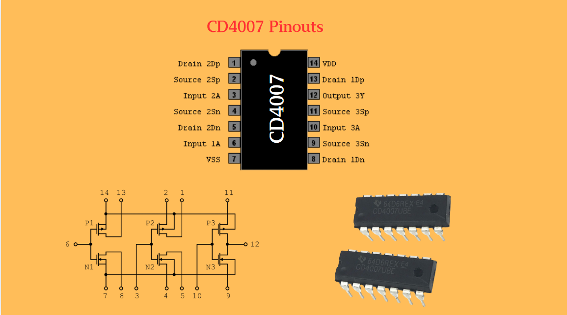
CD4007: A Comprehensive Analysis of a Multifunctional CMOS Integrated Circuit
In the field of modern electronic technology, CMOS (Complementary Metal-Oxide-Semiconductor) integrated circuits have become core components in digital and analog circuit design due to their low power consumption, high integration, and excellent compatibility. As a classic CMOS device, the CD4007 oc...
-
2025 / 07 / 07
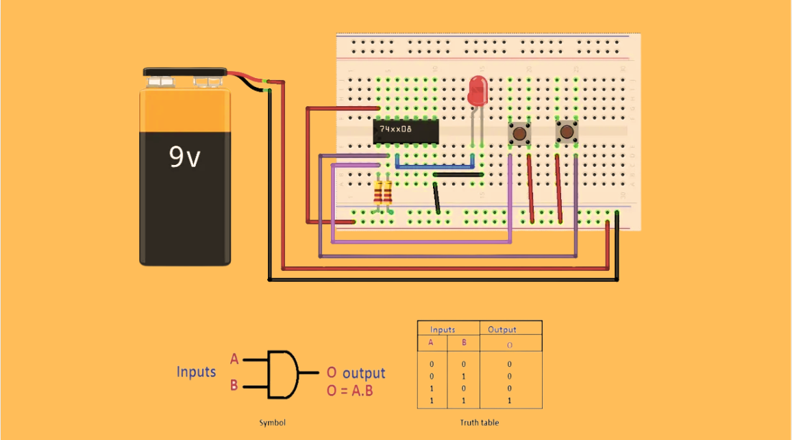
Understanding IC 7408: A Fundamental Component in Digital Logic Design
In the vast and intricate realm of digital electronics, integrated circuits (ICs) serve as the building blocks that enable the creation of complex and powerful systems. Among these, the IC 7408 holds a special place as a fundamental component in digital logic design. This article aims to provide a c...
-
2025 / 07 / 04
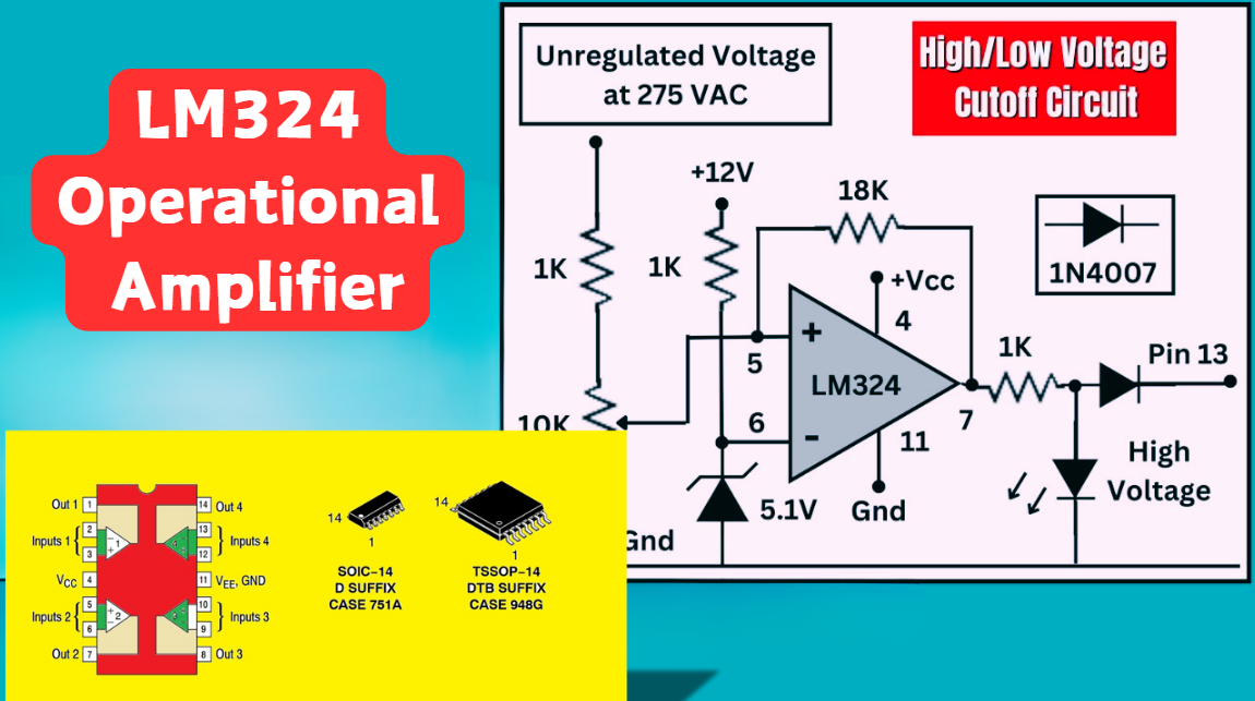
LM324 Operational Amplifier Comprehensive Guide: Pins, Applications, Packaging, and Datasheet
The LM324 is a low-cost integrated circuit featuring four independent operational amplifiers (op-amps), renowned for its wide voltage adaptability, low power consumption, and high reliability in industrial and consumer electronics. With a single-supply voltage range of 3V to 32V (or dual-supply rang...
-
2025 / 07 / 02
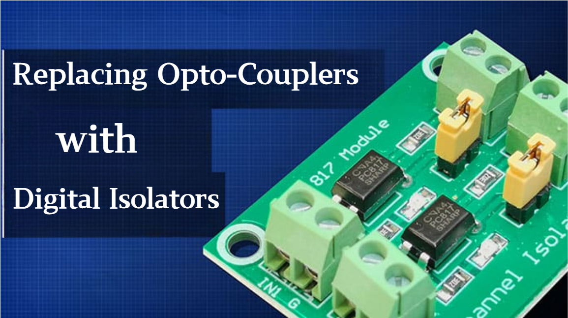
A Comprehensive Guide to Replacing Opto-Couplers with Digital Isolators: From Principles to Practice
In the ever-evolving landscape of electronic design, the transition from opto-couplers to digital isolators marks a pivotal shift in isolation technology. For decades, opto-couplers have been the cornerstone of electrical isolation in industrial control, medical devices, and power systems, relying o...
-
2025 / 06 / 30
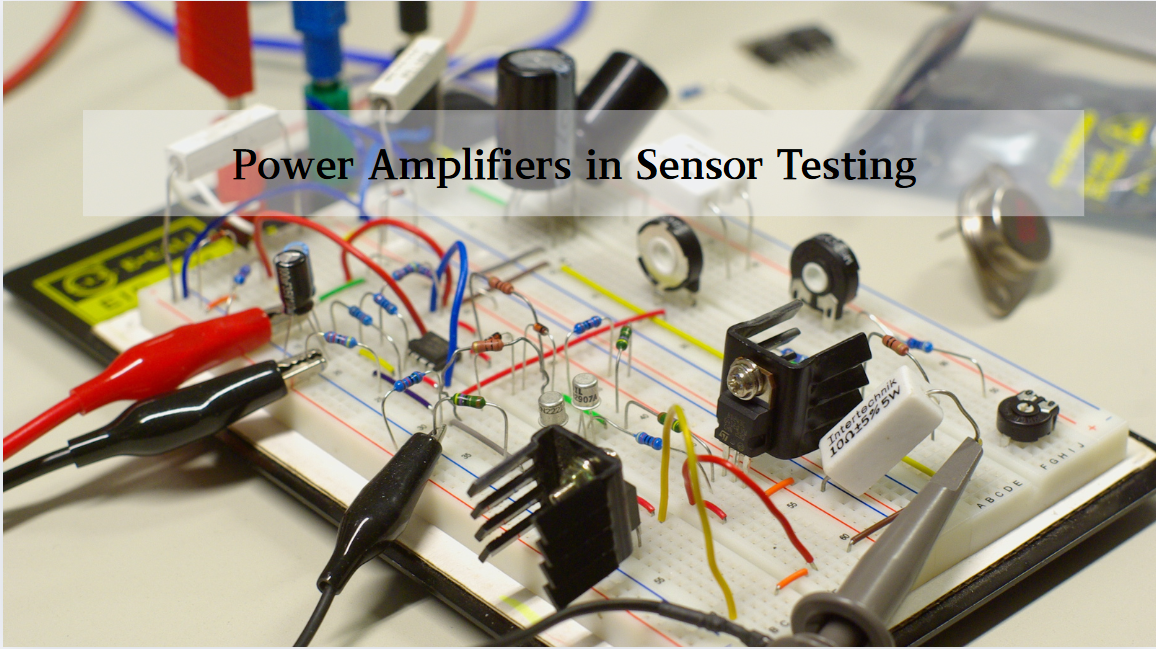
Multivariate Application Analysis of Power Amplifiers in Sensor Testing
In the field of modern sensor testing, power amplifiers (PAs) serve as core components and play an indispensable role. From amplifying weak signals to simulating complex physical environments, power amplifiers provide solid guarantees for the precise testing of sensor performance through their uniqu...
-
2025 / 06 / 28
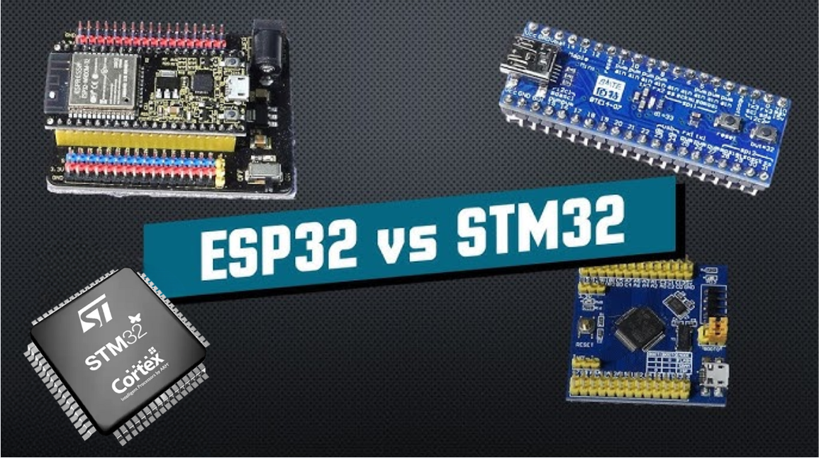
ESP32 vs STM32: Which Microcontroller Suits You Better?
In the field of embedded development, both ESP32 and STM32 are highly favored microcontrollers, each with unique features and advantages. When facing project development, how do you choose between them? This requires comprehensive consideration of multiple factors. The following detailed comparison ...
-
2025 / 06 / 26
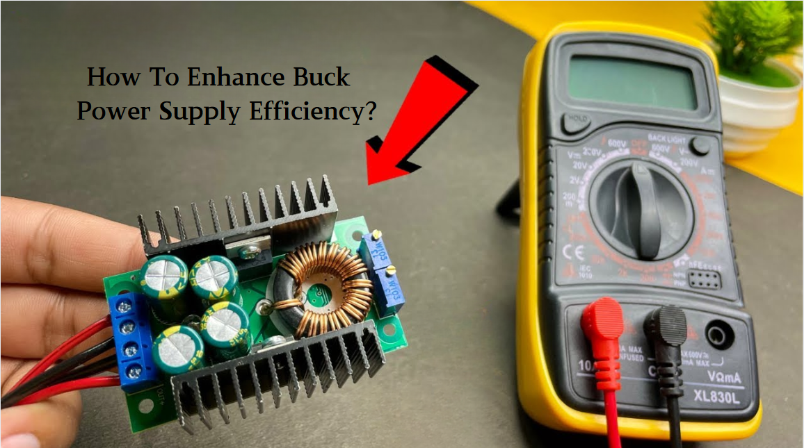
Key Strategies to Enhance Buck Power Supply Efficiency
Improving the efficiency of Buck (step-down) switching power supplies requires a multi-dimensional approach targeting energy loss sources, including component selection, topology optimization, control strategies, and thermal management. Below are core strategies and engineering practices:...
-
2025 / 06 / 26
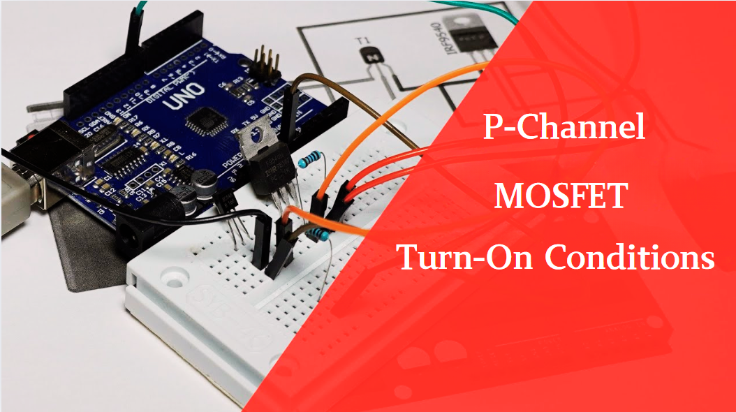
P-Channel MOSFET Turn-On Conditions
The turn-on conditions for a P-channel MOSFET (PMOS) are inverse to those of an N-channel MOSFET (NMOS), primarily governed by the relationship between the gate-source voltage (VGS) and the threshold voltage (Vth), along with voltage polarity. Here are the key points:A PMOS turns on when its gate vo...
-
2025 / 06 / 24
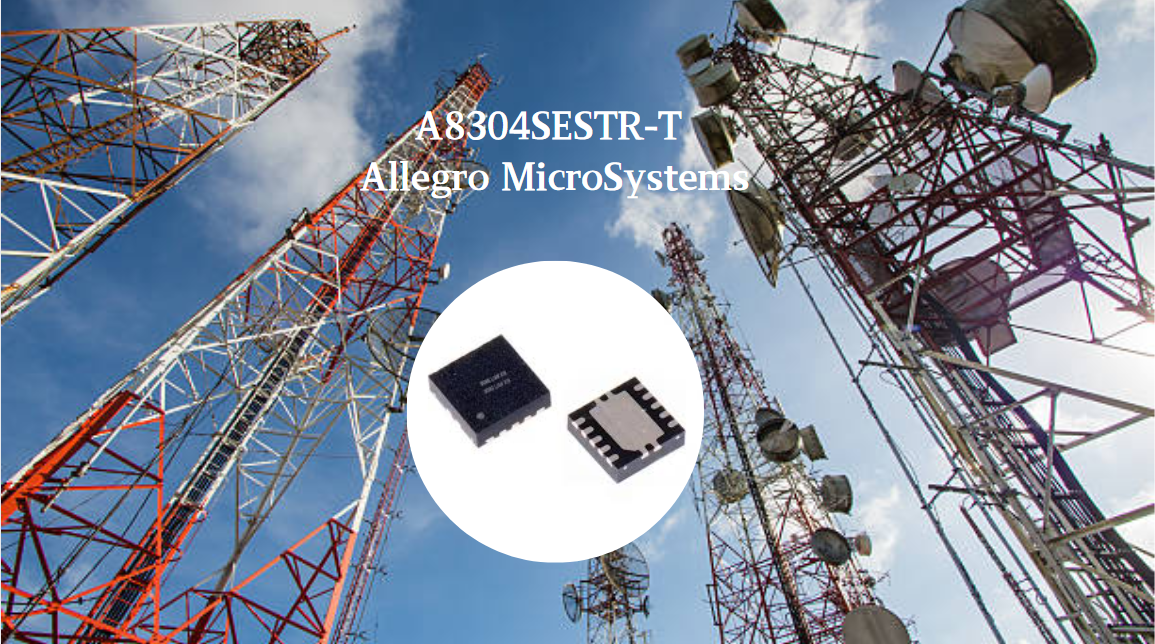
A8304SESTR-T Allegro MicroSystems-Single LNB Supply and Control Voltage Regulator
The Allegro MicroSystems A8304SESTR-T is a single-channel Low Noise Block Regulator (LNBR). It integrates a monolithic boost converter with MOSFET, current sensing, and compensation. Featuring a 704 kHz switching frequency, it uses few external components. With an I²C-compatible interface, it offers...
-
2025 / 06 / 20
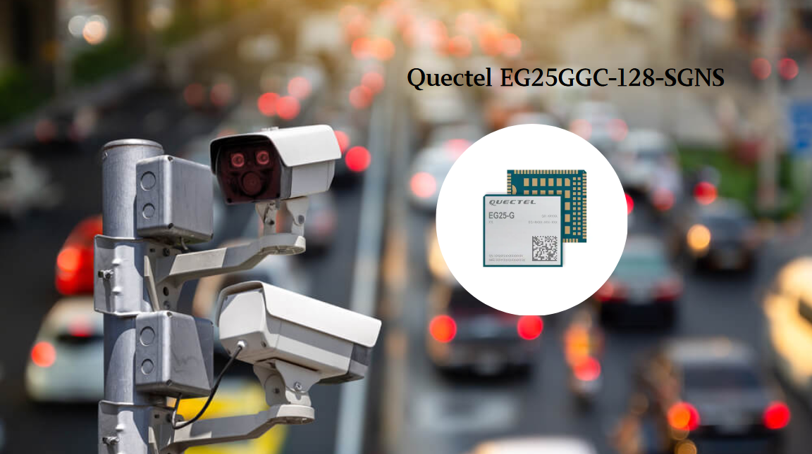
EG25GGC-128-SGNS by Quectel Wireless Solutions Co., Ltd: Features,Symbol,Footprint and Datasheet
The Quectel EG25GGC - 128 - SGNS is an LTE Cat 4 module optimized for M2M and IoT. Supporting 3GPP Rel. 11, it offers up to 150Mbps downlink and 50Mbps uplink. With global LTE/UMTS/GSM coverage, it's backward - compatible with EDGE/GPRS. Featuring multi - constellation GNSS (GPS, GLONASS, BeiDou, et...

2000+
Daily average RFQ Volume

30,000,000
Standard Product Unit

2800+
Worldwide Manufacturers

15,000 m2
In-stock Warehouse
 Wishlist (0 Items)