

- RFQ
- BOM
-
Contact Us
Tel: +86-0755-83501315
Email: sales@sic-components.com


- Chinese
- English
- French
- German
- Portuguese
- Spanish
- Russian
- Japanese
- Korean
- Arabic
- Irish
- Greek
- Turkish
- Italian
- Danish
- Romanian
- Indonesian
- Czech
- Afrikaans
- Swedish
- Polish
- Basque
- Catalan
- Esperanto
- Hindi
- Lao
- Albanian
- Amharic
- Armenian
- Azerbaijani
- Belarusian
- Bengali
- Bosnian
- Bulgarian
- Cebuano
- Chichewa
- Corsican
- Croatian
- Dutch
- Estonian
- Filipino
- Finnish
- Frisian
- Galician
- Georgian
- Gujarati
- Haitian
- Hausa
- Hawaiian
- Hebrew
- Hmong
- Hungarian
- Icelandic
- Igbo
- Javanese
- Kannada
- Kazakh
- Khmer
- Kurdish
- Kyrgyz
- Latin
- Latvian
- Lithuanian
- Luxembou..
- Macedonian
- Malagasy
- Malay
- Malayalam
- Maltese
- Maori
- Marathi
- Mongolian
- Burmese
- Nepali
- Norwegian
- Pashto
- Persian
- Punjabi
- Serbian
- Sesotho
- Sinhala
- Slovak
- Slovenian
- Somali
- Samoan
- Scots Gaelic
- Shona
- Sindhi
- Sundanese
- Swahili
- Tajik
- Tamil
- Telugu
- Thai
- Ukrainian
- Urdu
- Uzbek
- Vietnamese
- Welsh
- Xhosa
- Yiddish
- Yoruba
- Zulu
- Kinyarwanda
- Tatar
- Oriya
- Turkmen
- Uyghur
- Tag List
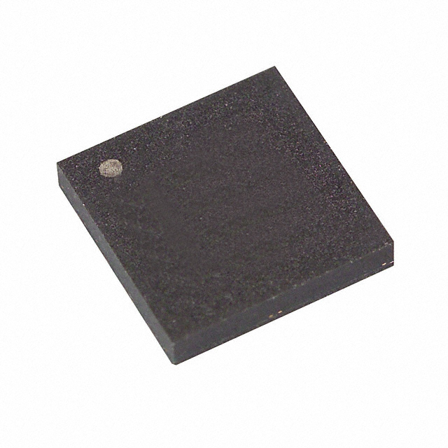
- 2.5D Integrated Circuits: The Fundamental Architectural Innovation for the Computing Power Revolution in Data Centers
2.5D Integrated Circuits: The Fundamental Architectural Innovation for the Computing Power Revolution in Data Centers
I. Computing Power Dilemmas in Data Centers and the Breakthrough Path of 2.5D ICs
Driven by AI training and large-scale data processing, modern data centers face three core challenges: a surge in computing density (single-server power consumption exceeding 5kW), memory wall bottlenecks (memory access latency accounting for 70% of computing time), and pressure to improve energy efficiency (Power Usage Effectiveness (PUE) needs to drop from 1.5 to below 1.1). Traditional 2D packaging (single-die integration) struggles to meet demands due to long interconnection distances (millimeter-scale) and high power consumption (30% of energy used for signal transmission); 3D stacking (e.g., vertical integration of High Bandwidth Memory (HBM)) shortens links but has excessively high thermal density (200W/cm²), requiring liquid cooling support. 2.5D integrated circuits, with their architecture of horizontal heterogeneous integration + short-distance interconnection, have become the key path for data centers to shift from "performance stacking" to "energy efficiency collaboration."
II. Technical Architecture of 2.5D ICs: Interposers Restructuring Collaboration Among Computing Units
The core of 2.5D ICs is the silicon interposer—an ultra-thin silicon substrate (thickness < 100μm) covered with microbumps (pitch < 50μm) and Through-Silicon Vias (TSVs), which can horizontally splice heterogeneous Chiplets (such as CPUs, GPUs, HBM, and FPGAs) to form "computing building blocks." Compared with traditional PCB interconnections, its advantages are reflected in:
Interconnection efficiency: Signal transmission distance is reduced from centimeter-scale to micrometer-scale, reducing latency by 80% (e.g., NVIDIA H100, through CoWoS packaging, reduces the communication latency between GPU and HBM3 from 100ns to 15ns);
Heterogeneous integration: Supports co-packaging of 5nm logic chips (e.g., AMD EPYC CPUs) and 28nm I/O chips (e.g., PCIe switches), improving yield by 25% (avoiding the risk of full advanced-process tape-out);
Thermal optimization: Chiplets are arranged side by side rather than vertically stacked, reducing thermal density by 40%, and the top heat sink can dissipate over 97% of heat (simulations show junction temperature fluctuations < 2℃).
Typical architecture case: TSMC's CoWoS-S technology integrates AI chips with 6-layer HBM3 on a silicon interposer, achieving 3.35TB/s bandwidth and 22% lower power consumption than 2D solutions, supporting large-scale deployment of NVIDIA A100/A800 in data centers.
III. Core Value of 2.5D ICs: The "Energy Efficiency Multiplier" of Data Centers
1. Breaking the Memory Wall: Close Collaboration Between HBM and Computing Chiplets
Memory access energy consumption accounts for over 40% of data centers. 2.5D ICs restructure storage architectures through high-speed interconnections between Chiplets. For example, AMD Instinct MI300 co-packages CPUs, GPUs, and HBM3 on an interposer, achieving a memory bandwidth of 5.2TB/s—40 times higher than PCIe 5.0 (128GB/s)—and increasing AI training speed by 30%. Microchip's Gen 5 PCIe switches (e.g., META-DX2C) further optimize internal interconnections in data centers, supporting 800G AEC cables and improving fiber bandwidth utilization by 50% with Lambda Splitting technology.
2. Computing Power Modularization: Plug-and-Play Ecosystem of Chiplets
2.5D ICs have spawned a "Chiplet economy": designers can combine dedicated Chiplets (e.g., AI acceleration Chiplets, security encryption Chiplets) on demand without redesigning the entire SoC. For example, Xilinx (now AMD)'s Versal AI Core integrates 7nm computing Chiplets and 22nm I/O Chiplets through an interposer, shortening the development cycle by 50%. Data center operators can iterate systems by replacing a single Chiplet (e.g., upgrading to HBM4) at a cost of only 1/3 of replacing the entire chip.
3. Power Efficiency Optimization: Collaborative Design of High-Density PMICs
For every 1% improvement in power efficiency of data center servers, annual electricity consumption is reduced by 120 million kWh. 2.5D packaging allows power management ICs (e.g., Microchip MCP16701) to be placed close to computing Chiplets; 8-channel parallel buck converters reduce power supply latency to 1μs, and 配合 I2C dynamic voltage regulation (12.5mV step), energy efficiency ratio is improved by 9%. Experiments show that AI servers using 2.5D power solutions reduce full-load power consumption from 4.8kW to 4.3kW.
IV. Engineering Challenges and Evolution Directions of 2.5D ICs
1. Testing and Yield: Core Thresholds for Mass Production
Silicon interposers contain millions of microbumps; any short circuit/open circuit will cause the entire package to fail. The industry uses pre-bonding testing (e.g., BIST architecture in IEEE 1149.1 standard) to detect TSV defects in interposers before Chiplet mounting, increasing yield from the initial 60% to 92% (TSMC 2024 data). In addition, hybrid bonding technology (e.g., Intel Foveros Direct) reduces bump pitch to 3μm, requiring sub-micron testing accuracy and driving the popularization of X-ray 3D inspection equipment.
2. Heat Dissipation and Materials: Coping with Rising Power Density
Although 2.5D thermal density is lower than 3D, AI chip power consumption has reached 700W (e.g., H100), and the thermal conductivity bottleneck of traditional silicon interposers has become apparent. The industry is exploring glass interposers (Coefficient of Thermal Expansion (CTE) = 3ppm/℃, close to silicon); although their thermal conductivity is low (1.1W/m·K), embedding copper pillars (thermal conductivity 400W/m·K) can improve heat dissipation efficiency by 18% (Intel 2025 test data). Meanwhile, liquid cooling plates directly contact the package top surface to control junction temperature below 85℃, meeting the 24/7 operation requirements of data centers.
3. Standardization and Ecosystem: From Technology to Industry
The UCIe 1.1 standard unifies Chiplet interfaces; AMD, NVIDIA, and other companies have opened Chiplet libraries to promote "LEGO-style design." Domestic Changdian Technology's XDFOI 2.5D technology has mass-produced 4nm Chiplets, and Tongfu Microelectronics has achieved 7nm packaging, but high-end hybrid bonding equipment still relies on imports. With the commissioning of domestic interposer production lines (e.g., SMIC Tianjin factory), the cost of domestic 2.5D packaging is expected to drop by 35% in 2025, accelerating domestic substitution in data centers.
V. 2.5D IC Application Cases in Data Center Scenarios
Application Scenarios 2.5D IC Solutions Performance Improvement
AI training clusters NVIDIA H100 (CoWoS packaging + HBM3) Computing density of 2.7 petaFLOPS/L
Supercomputing storage nodes AMD MI300 (co-packaged CPU+GPU+HBM) 42% reduction in storage access energy consumption
Edge data centers Microchip LAN9646+dsPIC33A (power + control) 60% reduction in 10GbE switch volume
High-density servers Intel EMIB technology (CPU+IO Chiplets) 45% reduction in motherboard area
VI. Future Trends: From 2.5D to "Multi-Dimensional Integration"
Mainstream adoption of Chiplet architecture: Yole predicts that 80% of high-end chips in data centers will adopt Chiplet designs by 2027, supporting flexible expansion and customization;
Heterogeneous material integration: Co-packaging of silicon, silicon carbide (SiC), and photonic chips to achieve optoelectronic integration (e.g., for data center optical interconnections);
Self-healing intelligent packaging: Integrating sensors and microcontrollers to monitor interconnection health in real time, with fault self-healing response time < 100μs.
Conclusion
2.5D integrated circuits, through interposer-based heterogeneous integration, achieve an optimal balance among computing power, power consumption, and cost. From NVIDIA's AI acceleration to Microchip's power optimization, from silicon interposers to glass substrates, this technology is reshaping the "underlying framework" of data centers. As the Chiplet ecosystem matures and testing technologies break through, 2.5D ICs will become the core engine for data centers to transition from "usable" to "efficient" in the next decade.

Hot Products
View More-

M29W160EB70ZA6 STMicroelectronics
-
74LVX174MTR STMicroelectronics
-
MC3303PW Texas Instruments
-
MCP6283T-E/MS Microchip Technology
-
SN74AVC4T245DR Texas Instruments
-
MAX5308EUE+ Analog Devices Inc./Maxim Integrated
-

CY2309ZXC-1H Infineon Technologies
-
COP8CDR9HVA8/NOPB Texas Instruments
-
EL5203IYZ Renesas Electronics America Inc
-
S-1200B46-I6T2G ABLIC Inc.
-
74FCT162652ATPVCG4 Texas Instruments
-
X40415V8I-CT1 Renesas Electronics America Inc
Related Blogs
-
2025 / 08 / 01
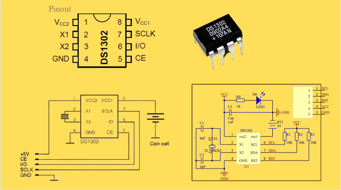
DS1302 RTC: Datasheet,Attributes,Features,Applications
As a low-power device widely used in electronic equipment, the DS1302 is centered on accurate real-time clock/calendar recording functions. It supports full-dimensional tracking of seconds, minutes, hours, days, weeks, months, and years, features automatic leap year compensation, and is compatible w...
-
2025 / 07 / 30
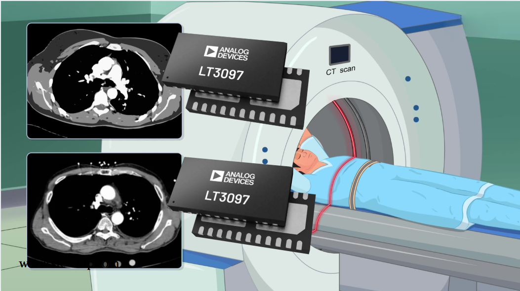
LT3097 Dual 500 mA, positive/negative, ultralow noise, ultrahigh PSRR low dropout linear regulator
The LT3097 is a dual, positive and negative, high-performance, low-dropout linear regulator featuring Analog Devices, Inc., ultralow noise and ultra-high power supply rejection ratio (PSRR) architecture for powering noise-sensitive applications. Each regulator delivers up to 500 mA with a typical 26...
-
2025 / 07 / 28
What is a Digital Integrated Circuit?
In the fast - paced world of modern electronics, digital integrated circuits (ICs) are the unsung heroes that power everything from our smartphones and laptops to complex supercomputers and industrial control systems. But what exactly is a digital integrated circuit?...
-
2025 / 07 / 25
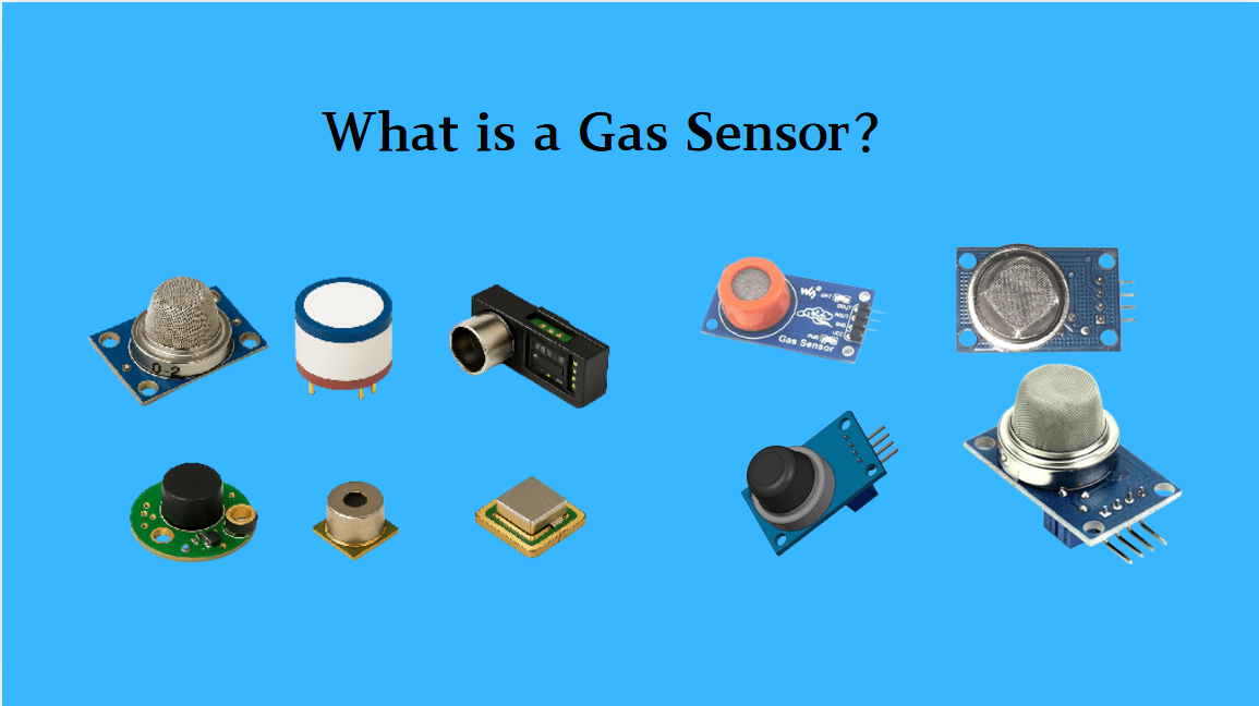
What is a Gas Sensor?
A gas sensor is a device that can convert information such as the composition and concentration of gas into electrical signals recognizable by electronic equipment. It is like the "olfactory organ" of an electronic system, capable of acutely detecting the presence of specific gases in the environmen...
-
2025 / 07 / 24
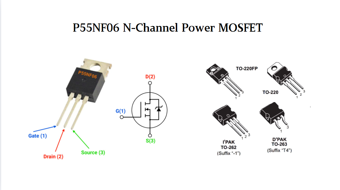
P55NF06 N-Channel Power MOSFET: Everything You Need To Know
In the vast landscape of semiconductor devices, MOSFETs (Metal - Oxide - Semiconductor Field - Effect Transistors) play a pivotal role, especially in power electronics. Among the numerous MOSFET models available, the P55NF06 stands out for its unique combination of features, making it suitable for a...
-
2025 / 07 / 23
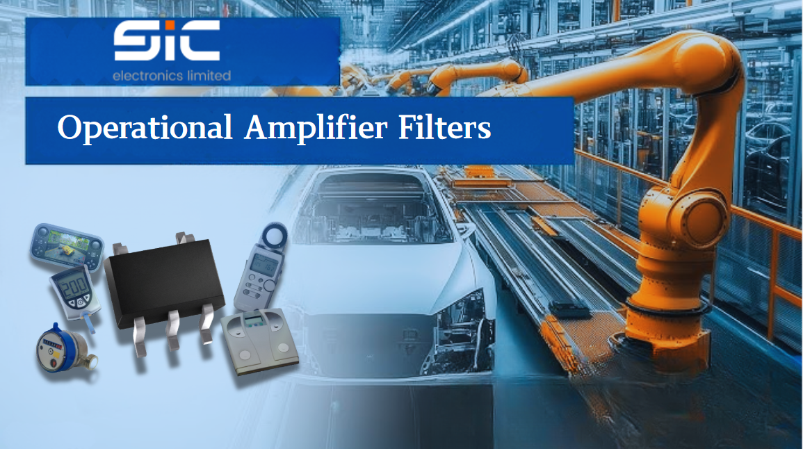
Operational Amplifier Filters: A Comprehensive Analysis from Fundamentals to Applications
In electronic systems, the purity and accuracy of signals directly determine the performance of devices. Electronic filters composed of operational amplifiers (op-amps) have become a "bridge" connecting original signals and valid information, thanks to their ability to precisely filter signal freque...
-
2025 / 07 / 19
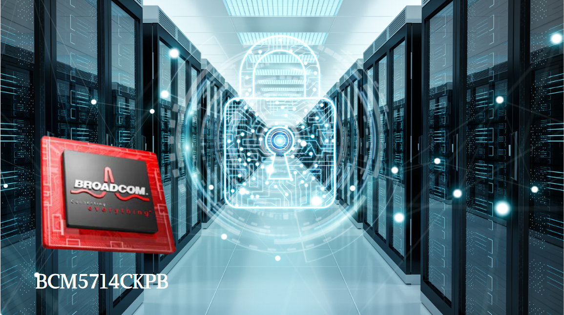
Broadcom BCM5714CKPB: Featrues,Applications,Datasheet And Advantages
When it comes to reliable, high-performance network connectivity in enterprise and industrial systems, the Broadcom BCM5714CKPB stands as a standout solution. This dual-port Gigabit Ethernet controller, developed by Broadcom—a leader in semiconductor innovation—combines robust features, versatile co...
-
2025 / 07 / 15
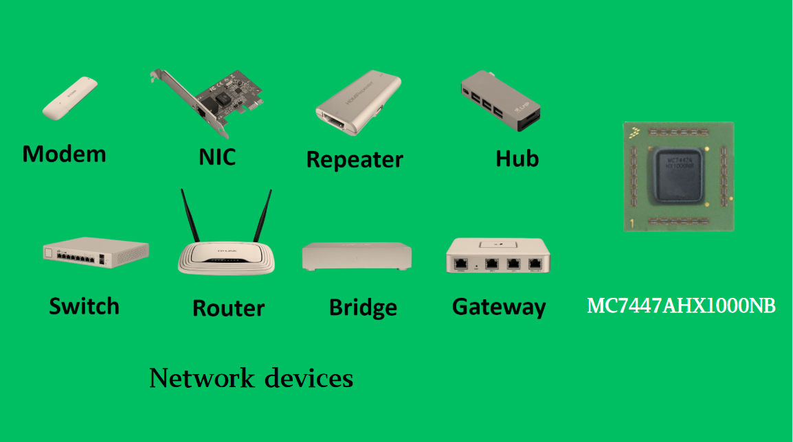
MC7447AHX1000NB: Technical Analysis and Applications of a High-Performance PowerPC Architecture Proc
In the field of embedded computing and network systems, the performance, energy efficiency, and compatibility of processors are often crucial to the success of a design. The MC7447AHX1000NB launched by NXP (formerly Freescale), as an important member of the MPC7447A series, has become an ideal choic...
-
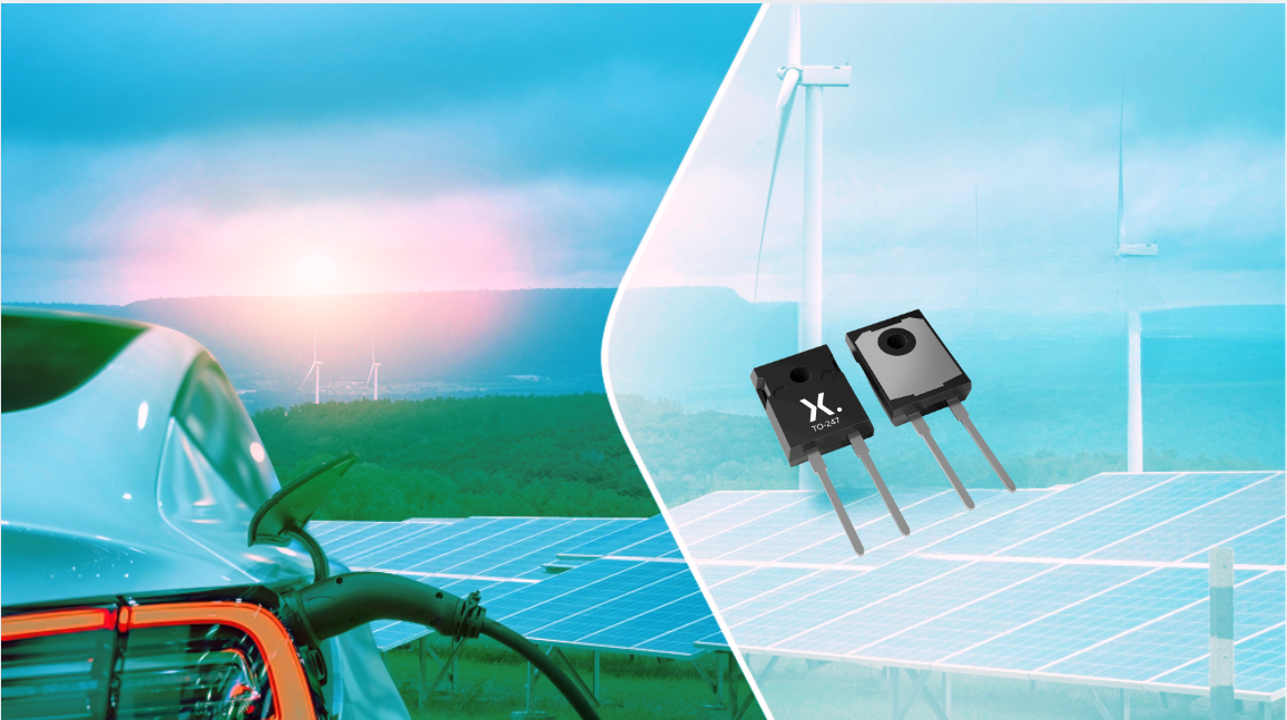
2025 / 07 / 14
Nexperia Unveils New 1200V/20A SiC Schottky Diodes to Empower Efficient Industrial Power Innovations
Nexperia recently announced the addition of two new 1200V, 20A silicon carbide (SiC) Schottky diodes—PSC20120J and PSC20120L—to its power electronics portfolio, further expanding its product landscape in high-performance semiconductors. Specifically designed to address the increasingly stringent dem...
-
2025 / 07 / 09
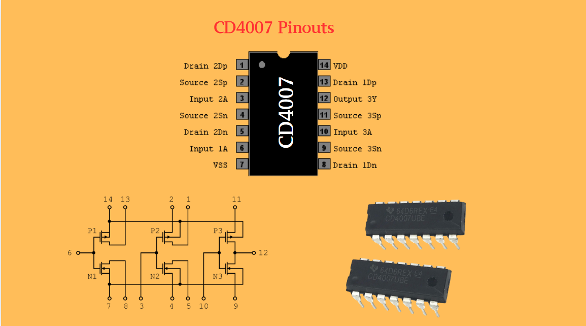
CD4007: A Comprehensive Analysis of a Multifunctional CMOS Integrated Circuit
In the field of modern electronic technology, CMOS (Complementary Metal-Oxide-Semiconductor) integrated circuits have become core components in digital and analog circuit design due to their low power consumption, high integration, and excellent compatibility. As a classic CMOS device, the CD4007 oc...

2000+
Daily average RFQ Volume

30,000,000
Standard Product Unit

2800+
Worldwide Manufacturers

15,000 m2
In-stock Warehouse
 Wishlist (0 Items)