

- RFQ
- BOM
-
Contact Us
Tel: +86-0755-83501315
Email: sales@sic-components.com


- Chinese
- English
- French
- German
- Portuguese
- Spanish
- Russian
- Japanese
- Korean
- Arabic
- Irish
- Greek
- Turkish
- Italian
- Danish
- Romanian
- Indonesian
- Czech
- Afrikaans
- Swedish
- Polish
- Basque
- Catalan
- Esperanto
- Hindi
- Lao
- Albanian
- Amharic
- Armenian
- Azerbaijani
- Belarusian
- Bengali
- Bosnian
- Bulgarian
- Cebuano
- Chichewa
- Corsican
- Croatian
- Dutch
- Estonian
- Filipino
- Finnish
- Frisian
- Galician
- Georgian
- Gujarati
- Haitian
- Hausa
- Hawaiian
- Hebrew
- Hmong
- Hungarian
- Icelandic
- Igbo
- Javanese
- Kannada
- Kazakh
- Khmer
- Kurdish
- Kyrgyz
- Latin
- Latvian
- Lithuanian
- Luxembou..
- Macedonian
- Malagasy
- Malay
- Malayalam
- Maltese
- Maori
- Marathi
- Mongolian
- Burmese
- Nepali
- Norwegian
- Pashto
- Persian
- Punjabi
- Serbian
- Sesotho
- Sinhala
- Slovak
- Slovenian
- Somali
- Samoan
- Scots Gaelic
- Shona
- Sindhi
- Sundanese
- Swahili
- Tajik
- Tamil
- Telugu
- Thai
- Ukrainian
- Urdu
- Uzbek
- Vietnamese
- Welsh
- Xhosa
- Yiddish
- Yoruba
- Zulu
- Kinyarwanda
- Tatar
- Oriya
- Turkmen
- Uyghur
ICs for AI Applications
Today, as large model parameters exceed one trillion, AI chips have transcended traditional semiconductors to become the core infrastructure driving the intelligent revolution. From supercomputing clusters for cloud training to real-time inference on edge devices, AI chips are redefining computing paradigms through architectural innovation, process evolution, and ecosystem building. The global AI chip market size will exceed $80 billion by 2025, with a compound annual growth rate of 32%, and its technological evolution spans the entire chain from algorithm adaptation to scenario implementation.
I. Architectural Revolution: A Paradigm Shift from General-Purpose to Specialized
The essence of AI chips is computing engines tailored for neural network algorithms. Their architectural innovation revolves around "data parallelism" and "energy efficiency ratio," forming four technical schools:
1. Parallel Pioneers: Large-Scale Evolution of GPUs
NVIDIA’s Blackwell architecture GPUs (e.g., B200) allocate over 80% of transistors to computing units, integrating 1.4 trillion transistors per chip. With 32,768 CUDA cores, they achieve 2.3 Pflops of FP16 computing power. Unlike CPUs with serial instruction processing, GPUs use a "Single Instruction Multiple Data (SIMD)" architecture, improving the efficiency of core neural network operations such as matrix multiplication and convolution by 40x. The 2025-released GB200 integrates a Grace CPU, building an integrated "computing-storage-communication" superchip system through 288GB/s memory bandwidth and 16TB/s NVLink interconnection, designed specifically for training trillion-parameter models.
2. Flexible Innovators: Scenario-Based Adaptation of FPGAs
Xilinx (now AMD)’s AI Engine series combines programmable logic units (LUT+FF) with dedicated DSPs to achieve "hardware pipelines + dynamic task scheduling" in autonomous driving domain controllers. For example, Mobileye EyeQ6H uses a 12nm FPGA to support real-time processing of 12 camera feeds with latency < 10ms and power consumption of only 25W. Its advantage lies in enabling algorithm iteration without redesigning the chip, making it suitable for rapid verification of ADAS systems. However, programming complexity and cost limit its popularity in consumer applications.
3. Energy Efficiency Champions: Extreme Customization of ASICs
Google TPU v5 uses a "systolic array + on-chip memory" architecture to boost matrix operation energy efficiency to 300 TOPS/W (INT8), 15x that of GPUs. Cambricon MLU370 adopts Chiplet technology, integrating 32 AI cores and HBM2e memory to achieve 1.2TB/s bandwidth in large model inference, supporting real-time parsing of Transformer models with over 100 layers. By 固化 neural network operators (e.g., convolution, Softmax), these chips deliver "TOPS-level computing power in millimeter-scale packaging" for scenarios such as autonomous driving (Horizon Journey 6) and smartphones (Apple A17 Pro’s NPU).
4. Future Explorations: Neuromorphic and Memory-Computing Integration
IBM TrueNorth Generation 2 chips simulate biological synaptic structures, with 4,096 neurons and 100 million synapses, achieving 1 million pulses per second of event-driven computing at 100mW power consumption, suitable for drone visual perception. Memory-computing integration technology breaks through the von Neumann bottleneck: for instance, Zhicun Technology’s memory-computing chips achieve 128TOPS/W (INT4) at 1.5V, already used in smartwatch heart rate anomaly detection, reducing power consumption by 90% compared to traditional solutions.
II. Scenario Differentiation: Computing Ecosystems for Cloud and Edge
AI chip design logic varies by deployment scenario, forming a dual-track evolution of "cloud prioritizing computing power, edge prioritizing energy efficiency":
1. Cloud: Computing Foundation of the Large Model Era
Training chips must meet three core requirements: high precision (FP32/BF16), high bandwidth (HBM3), and scalability (multi-card interconnection). NVIDIA H100 accelerates BERT model training by 30x via its Transformer Engine; Huawei Ascend 910C uses 2x 910B chips interconnected via D2D, enabling 384-chip collaboration in the CloudMatrix 384 supernode to support trillion-parameter optimization of the Pangu large model. For inference, Cambricon MLU370’s sparse computing acceleration technology reduces large model inference latency by 40% and costs by 50%, now fully deployed on Alibaba Cloud.
2. Edge: Real-Time Response for Edge Intelligence
Edge chips focus on energy efficiency ratio (TOPS/W) and real-time performance (millisecond-level latency). Apple A17 Pro’s 16-core NPU delivers 30TOPS (INT8) at 2.5W, supporting real-time ProRes video generation; Horizon Journey 6 completes full-scenario perception for urban NOA at 8W power consumption with latency < 5ms via Dynamic Voltage and Frequency Scaling (DVFS). Notably, edge chips are evolving from "single computing power" to "scenario customization": for example, T-Head HanGuang 800 integrates dedicated image encoding/decoding units, enabling face recognition in security cameras at only 0.8W power consumption.
III. Key Features: Systematic Breakthroughs from Architecture to Ecosystem
AI chip competitiveness lies in the synergistic optimization of a "computing-storage-software" trinity:
1. Multi-Precision Computing Engines
Support for dynamic precision switching from FP32→INT8→INT4: NVIDIA B200’s FP8 tensor cores double training speed while maintaining model accuracy. Cambricon MLU270’s mixed-precision units (supporting FP16/INT8/INT4) automatically select optimal precision for edge inference, improving energy efficiency by 60%.
2. Technologies to Break the Memory Wall
A three-tier storage architecture combining HBM3 memory (4.8TB/s bandwidth), on-chip SRAM (e.g., TPU v5’s 32MB matrix memory), and CXL 3.0 protocol (latency < 100ns). Biren BR100 integrates 6x HBM2e stacks via Chiplet, achieving 1.6TB/s bandwidth to solve the "fast computing, slow data movement" bottleneck in large models.
3. Software-Defined Flexibility
NVIDIA CUDA, Huawei CANN, and Cambricon MagicMind form three major ecosystems, reducing developer barriers through operator libraries (supporting 500+ neural network layers) and automatic tuning. Baidu Kunlun X3 accelerates Wenxin Yiyan inference by 1.8x compared to GPUs via "model compilation + hardware acceleration."
IV. Challenges and Trends: From Performance Competition to Ecosystem Building
1. Energy Efficiency Bottlenecks and New Material Breakthroughs
Energy efficiency improvements in sub-7nm processes are slowing, making 3D packaging (TSMC CoWoS) and new devices (memory-computing integration, phase-change neurons) critical. By 2025, Samsung’s 1β-process memory-computing chips will achieve 500TOPS/W, suitable for real-time rendering in AR glasses.
2. Domestic Substitution and Ecosystem Closure
Huawei Ascend, Cambricon, and Horizon have formed "chip-toolchain-solution" closed loops. For example, Horizon Journey 6 achieves 85% computing power utilization in XPeng X9’s self-developed urban NOA, surpassing NVIDIA solutions by 20%. Domestic DCUs (e.g., Moore Threads MTT S80) accelerate industrial software migration via CUDA compatibility.
3. Integration of Security and Privacy Computing
Automotive AI chips (e.g., Black Sesame A2000) integrate Hardware Security Modules (HSM) to support model parameter encryption; federated learning-specific chips (e.g., Suyuan SuiSi 3.0) enable "data-local" privacy-preserving inference, meeting needs in sensitive scenarios like healthcare and finance.
V. Case Studies: Typical Practices from Cloud to Edge
Cloud Training: NVIDIA GB200+Grace superchips quadruple single-node computing power and reduce carbon emissions by 35% in Meta’s LLaMA3 training.
Intelligent Driving: Tesla FSD 4.0 chips (custom ASICs) integrate 256 AI cores, achieving 2000TOPS (INT8) via on-chip 10GB SRAM to support real-time multi-target tracking in urban roads.
Edge Innovation: Xiaomi Surge C2’s AI camera unit, via a dedicated Image Neural Processing Unit (AINPU), enables real-time 4K video noise reduction at 0.5W, outperforming traditional ISP solutions in image quality.
Conclusion: The Chip Philosophy of the Computing Power Inclusion Era
The evolution of AI chips is an ongoing dialogue between algorithmic needs and hardware capabilities. From GPU’s general parallelism to ASIC’s scenario customization, from cloud computing giants to edge energy-efficient spirits, each architectural innovation expands the boundaries of intelligence. As memory-computing integration breaks the von Neumann bottleneck and neuromorphic chips simulate biological intelligence, AI chips are transforming from "computing power providers" to "intelligent co-creators." In the next decade, a chip the size of a fingernail may carry city-level intelligent decision-making—all beginning with a rethinking of "the nature of computing": not chips adapting to algorithms, but algorithms growing from the genes of chips.

Hot Products
View More-
NCV7513FTR2G onsemi
-
ADR530BKS-R2 Analog Devices Inc.
-
MC1489ADR2G onsemi
-
24FC256-I/MF Microchip Technology
-
LTC8043ES8#TRPBF Analog Devices Inc.
-
EPF10K30ATI144-3N Intel
-
TL064BCDR Texas Instruments
-
24C00/SN Microchip Technology
-
AD7868AR-REEL Analog Devices Inc.
-
MC68376BAMAB20 NXP USA Inc.
-

SLE 88CF4000P MFC5.8 Infineon Technologies
-
MC9S08DV60CLH NXP USA Inc.
Related Blogs
-
2025 / 08 / 01
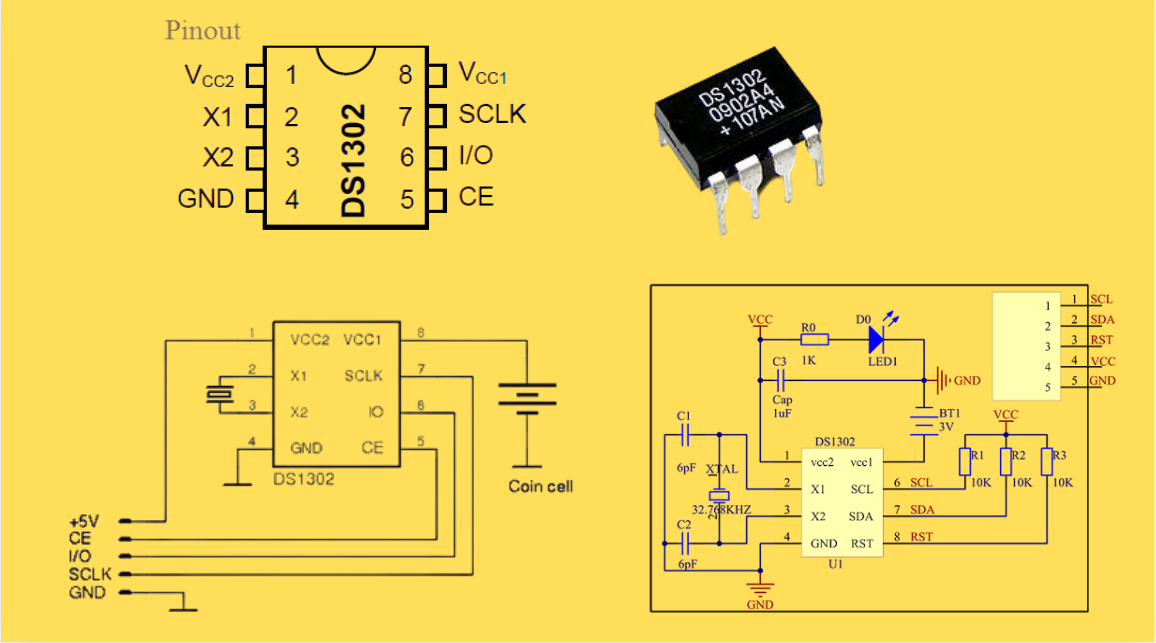
DS1302 RTC: Datasheet,Attributes,Features,Applications
As a low-power device widely used in electronic equipment, the DS1302 is centered on accurate real-time clock/calendar recording functions. It supports full-dimensional tracking of seconds, minutes, hours, days, weeks, months, and years, features automatic leap year compensation, and is compatible w...
-
2025 / 07 / 30
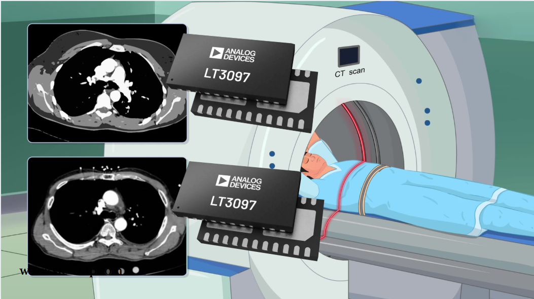
LT3097 Dual 500 mA, positive/negative, ultralow noise, ultrahigh PSRR low dropout linear regulator
The LT3097 is a dual, positive and negative, high-performance, low-dropout linear regulator featuring Analog Devices, Inc., ultralow noise and ultra-high power supply rejection ratio (PSRR) architecture for powering noise-sensitive applications. Each regulator delivers up to 500 mA with a typical 26...
-
2025 / 07 / 28
What is a Digital Integrated Circuit?
In the fast - paced world of modern electronics, digital integrated circuits (ICs) are the unsung heroes that power everything from our smartphones and laptops to complex supercomputers and industrial control systems. But what exactly is a digital integrated circuit?...
-
2025 / 07 / 25
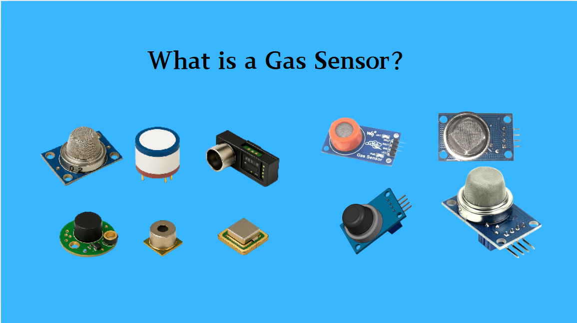
What is a Gas Sensor?
A gas sensor is a device that can convert information such as the composition and concentration of gas into electrical signals recognizable by electronic equipment. It is like the "olfactory organ" of an electronic system, capable of acutely detecting the presence of specific gases in the environmen...
-
2025 / 07 / 24
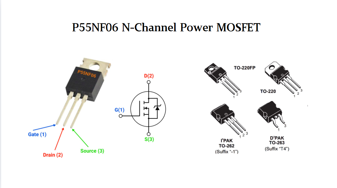
P55NF06 N-Channel Power MOSFET: Everything You Need To Know
In the vast landscape of semiconductor devices, MOSFETs (Metal - Oxide - Semiconductor Field - Effect Transistors) play a pivotal role, especially in power electronics. Among the numerous MOSFET models available, the P55NF06 stands out for its unique combination of features, making it suitable for a...
-
2025 / 07 / 23
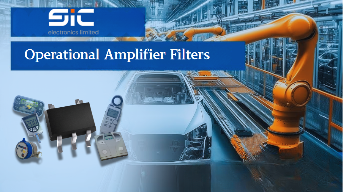
Operational Amplifier Filters: A Comprehensive Analysis from Fundamentals to Applications
In electronic systems, the purity and accuracy of signals directly determine the performance of devices. Electronic filters composed of operational amplifiers (op-amps) have become a "bridge" connecting original signals and valid information, thanks to their ability to precisely filter signal freque...
-
2025 / 07 / 19
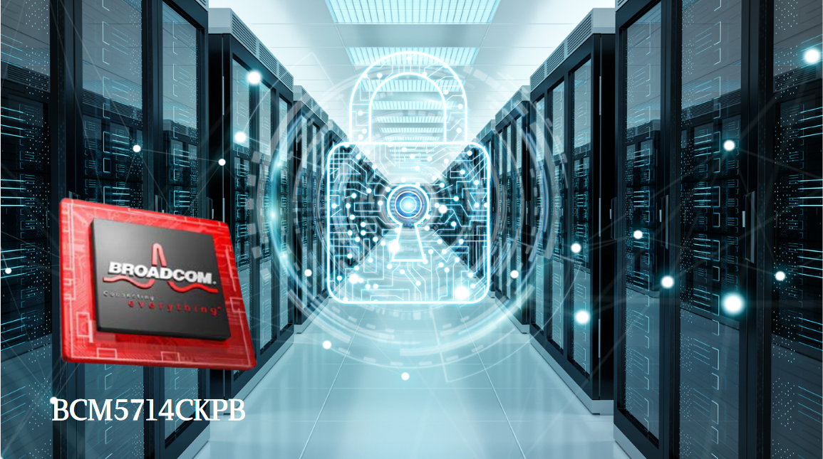
Broadcom BCM5714CKPB: Featrues,Applications,Datasheet And Advantages
When it comes to reliable, high-performance network connectivity in enterprise and industrial systems, the Broadcom BCM5714CKPB stands as a standout solution. This dual-port Gigabit Ethernet controller, developed by Broadcom—a leader in semiconductor innovation—combines robust features, versatile co...
-
2025 / 07 / 15
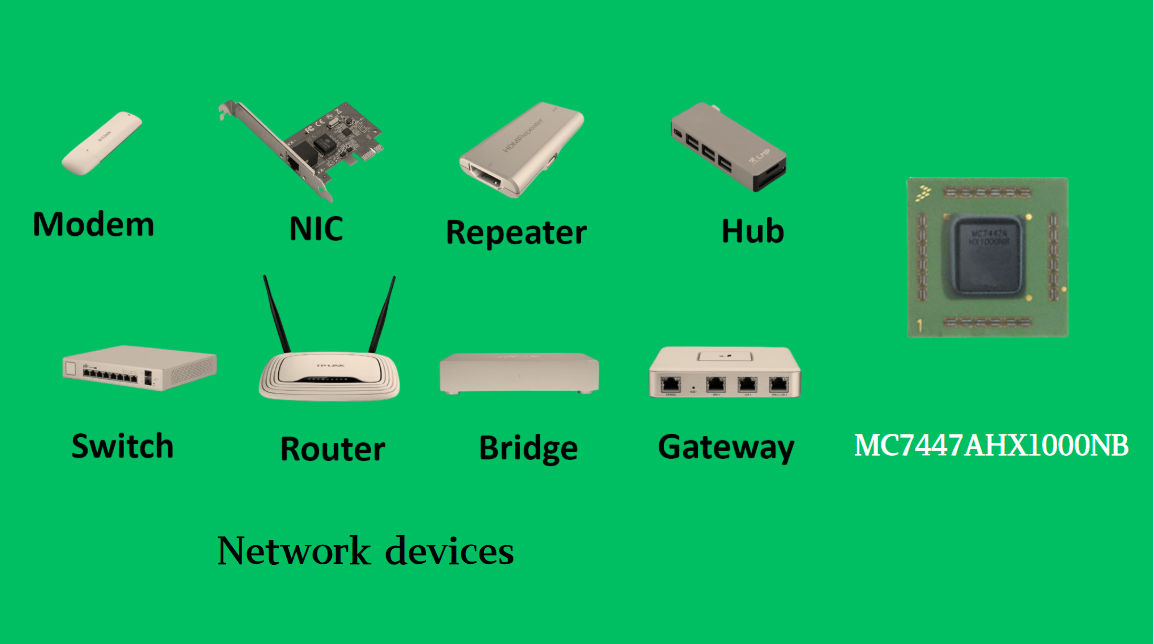
MC7447AHX1000NB: Technical Analysis and Applications of a High-Performance PowerPC Architecture Proc
In the field of embedded computing and network systems, the performance, energy efficiency, and compatibility of processors are often crucial to the success of a design. The MC7447AHX1000NB launched by NXP (formerly Freescale), as an important member of the MPC7447A series, has become an ideal choic...
-
2025 / 07 / 14
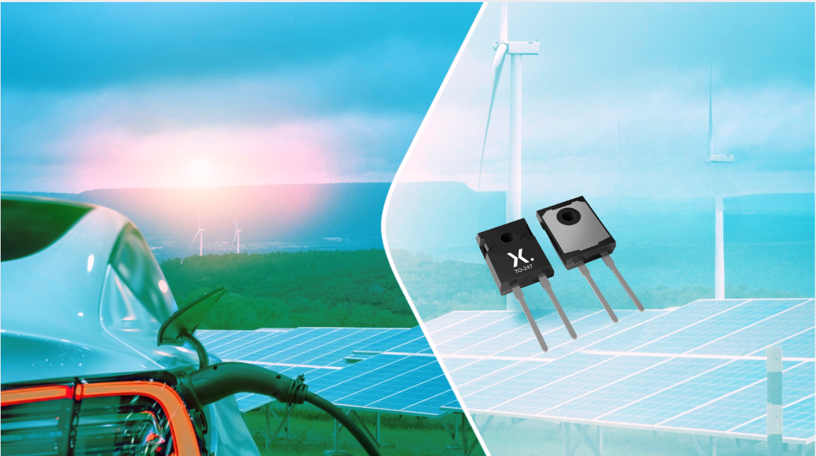
Nexperia Unveils New 1200V/20A SiC Schottky Diodes to Empower Efficient Industrial Power Innovations
Nexperia recently announced the addition of two new 1200V, 20A silicon carbide (SiC) Schottky diodes—PSC20120J and PSC20120L—to its power electronics portfolio, further expanding its product landscape in high-performance semiconductors. Specifically designed to address the increasingly stringent dem...
-
2025 / 07 / 09
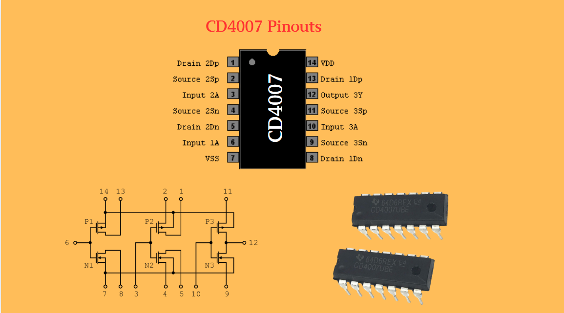
CD4007: A Comprehensive Analysis of a Multifunctional CMOS Integrated Circuit
In the field of modern electronic technology, CMOS (Complementary Metal-Oxide-Semiconductor) integrated circuits have become core components in digital and analog circuit design due to their low power consumption, high integration, and excellent compatibility. As a classic CMOS device, the CD4007 oc...

2000+
Daily average RFQ Volume

30,000,000
Standard Product Unit

2800+
Worldwide Manufacturers

15,000 m2
In-stock Warehouse
 Wishlist (0 Items)