- RFQ
- BOM
-
Contact Us
Tel: +86-0755-83501315
Email: sales@sic-components.com


- Chinese
- English
- French
- German
- Portuguese
- Spanish
- Russian
- Japanese
- Korean
- Arabic
- Irish
- Greek
- Turkish
- Italian
- Danish
- Romanian
- Indonesian
- Czech
- Afrikaans
- Swedish
- Polish
- Basque
- Catalan
- Esperanto
- Hindi
- Lao
- Albanian
- Amharic
- Armenian
- Azerbaijani
- Belarusian
- Bengali
- Bosnian
- Bulgarian
- Cebuano
- Chichewa
- Corsican
- Croatian
- Dutch
- Estonian
- Filipino
- Finnish
- Frisian
- Galician
- Georgian
- Gujarati
- Haitian
- Hausa
- Hawaiian
- Hebrew
- Hmong
- Hungarian
- Icelandic
- Igbo
- Javanese
- Kannada
- Kazakh
- Khmer
- Kurdish
- Kyrgyz
- Latin
- Latvian
- Lithuanian
- Luxembou..
- Macedonian
- Malagasy
- Malay
- Malayalam
- Maltese
- Maori
- Marathi
- Mongolian
- Burmese
- Nepali
- Norwegian
- Pashto
- Persian
- Punjabi
- Serbian
- Sesotho
- Sinhala
- Slovak
- Slovenian
- Somali
- Samoan
- Scots Gaelic
- Shona
- Sindhi
- Sundanese
- Swahili
- Tajik
- Tamil
- Telugu
- Thai
- Ukrainian
- Urdu
- Uzbek
- Vietnamese
- Welsh
- Xhosa
- Yiddish
- Yoruba
- Zulu
- Kinyarwanda
- Tatar
- Oriya
- Turkmen
- Uyghur
ICs for Data Centers
In the digital economy era, data centers carry 90% of the world’s computing demand, while integrated circuits (ICs), as their "neural center," are redefining computing density, energy efficiency boundaries, and system resilience through architectural innovation. From heterogeneous integration to memory-computing collaboration, from electrical interconnection to optical domain transmission, the evolution of data center ICs is essentially a continuous breakthrough in the "computing power-power consumption-cost" tripartite constraint.
I. Strategic Value: "Chip-Level Infrastructure" of Data Centers
The core contradiction of data centers—300% annual growth in computing demand versus PUE constraints below 1.15—has forced ICs to evolve from "functional components" to "system-level solutions." It is estimated that a high-performance AI chip can support the computing power of 200 traditional servers, while advanced packaging technologies can reduce rack energy consumption by 40%. The strategic value of this "chip-level infrastructure" is reflected in:
Revolution in computing density: 2.5D/3D packaging enables single-chip computing power to exceed 500 TOPS, increasing rack computing density to 3 petaFLOPS/L (10 times that of traditional solutions);
Reconstruction of energy efficiency ratio: Near-memory computing architecture reduces memory access energy consumption by 60%, lowering the cost per watt of computing power by 75%;
Enhanced system resilience: Chiplet modular design supports "plug-and-play" upgrades, shortening the hardware iteration cycle from 3 years to 6 months.
These breakthroughs directly impact data center TCO (Total Cost of Ownership): After adopting a heterogeneous integration solution, a supercomputing center saw annual operating costs drop by 28% and computing expansion efficiency increase by 4 times.
II. Chip Matrix: Full-Stack Layout from Computing to Interconnection
Data center ICs have formed four core clusters: "computing-storage-interconnection-management," with each cluster following the design logic of "specialization + collaboration":
1. Computing Engines: The Philosophy of Heterogeneous Acceleration
General computing (CPU): Intel Sierra Forest (144-core E-Core) achieves 240% improvement in performance per watt through Chiplet architecture, optimized for cloud-native lightweight tasks;
Parallel acceleration (GPU/TPU): Adopting SIMT/SIMD architecture, typical examples include NVIDIA H200 with 96GB HBM3e, achieving 819GB/s memory bandwidth to support large model training;
Dedicated acceleration (DPU/NPU): Marvell Prestera 98CX1132 DPU offloads 70% of network load; Cambrian MLU590 optimizes through sparse computing, reducing energy consumption for visual inference by 30%.
2. Storage Systems: Evolution from HBM to Memory-Computing Integration
High-bandwidth memory (HBM): 12-layer HBM3e has become the standard for AI chips, with bandwidth 10 times higher than DDR5, solving the "memory wall" bottleneck;
Memory-computing integration: Biren BR100’s on-chip cache hierarchical design reduces external memory access by 50%, lowering recommendation system latency by 45%;
Storage chipification: Micron CXL-DIMM embeds computing logic into memory, increasing database query speed by 10 times.
3. Interconnection Architecture: The Standard Battle of Three-Dimensional Communication
Chiplet interconnection (UCIe): 40Gbps Die-to-Die links support flexible Chiplet networking; TSMC CoWoS-S achieves 15ns latency (1/7 that of PCB);
Rack interconnection (224G Ethernet): Broadcom Tomahawk 5 switches integrate CEI-224G PHY, supporting 3.2Tbps bandwidth per chip with stable cross-rack latency of 2μs;
Optical domain expansion: Co-packaged optics (CPO) technology integrates lasers with switch chips, extending transmission distance beyond 100 meters and reducing power consumption by 35%.
4. Management Hub: The Last Line of Defense for Security and Energy Efficiency
Out-of-band management (BMC): Aspeed AST2600 BMC supports IPMI 2.0, enabling remote server firmware upgrades and power consumption monitoring;
Power management (PMIC): MPS SY85121 reduces full-load power consumption of AI servers to 4.3kW through dynamic voltage adjustment (12.5mV step);
Security chips (TPM): Infineon OPTIGA TPM 2.0 integrates hardware encryption to ensure data center key security.
III. Solutions: Collaborative Design from Chips to Systems
1. Rack-Level Heterogeneous Integration Solution
Adopting a "CPU+GPU+DPU" triple architecture: AMD MI300X co-packages 8-core Zen4, CDNA3 GPU, and 128GB HBM3, connecting to Marvell 800G optical modules via CXL 2.0 to achieve zero-copy collaboration between storage, network, and computing. Tests in an AI training cluster show that this solution increases 1000-card parallel efficiency by 22% and reduces synchronization latency by 18%.
2. High-Density Low-Power Design
Targeting rack space constraints (depth ≤30 inches), 2.5D packaging reduces volume: Intel EMIB technology horizontally splices CPU and IO chiplets, reducing motherboard area by 45%; Changdian Technology XDFOI mass-produces 4nm Chiplets, increasing single-chip integration by 3 times.
3. Optical-Electrical Hybrid Interconnection Architecture
In a 1600-square-foot standard computer room, deploying Broadcom 1.6T CPO switches and Synopsys UCIe IP to build a "electrical interconnection (intra-rack) + optical interconnection (inter-rack)" three-dimensional network. Test data shows that this architecture supports 3.2PB storage access in a 20-server cluster, with bandwidth utilization reaching 92%, 50% higher than traditional solutions.
IV. Technical Trends: Paradigm Shift from Performance to Sustainability
1. Architectural Evolution: Chiplet + Optoelectronic Co-Packaging
Yole predicts that 80% of high-end chips in data centers will adopt Chiplet designs by 2027. Heterogeneous co-packaging of silicon, silicon carbide, and photonic chips achieves optical interconnection latency <10ns, supporting the vision of an "on-chip data center."
2. Energy Efficiency Revolution: Near-Memory Computing + Self-Sensing Packaging
Intelligent packaging with integrated sensors monitors over 2 million microbumps in real time, with fault self-healing response <100μs; memory-computing integration architecture reduces visual algorithm energy consumption to 3.2W, breaking the von Neumann bottleneck.
3. Standard Collaboration: Ecosystem Construction of UCIe + CXL
UCIe 1.1 unifies chiplet interfaces, and CXL 3.0 enables memory pooling. Their collaboration promotes "computing power resourceization"—servers can dynamically call storage and acceleration resources in the cluster, increasing utilization from 30% to 75%.
Conclusion: The Future of Data Centers Defined by ICs
Competition in data center ICs essentially revolves around "system-level innovation capabilities"—from Intel’s E-Core energy efficiency revolution to NVIDIA’s HBM bandwidth breakthroughs, from Broadcom’s optical interconnection integration to Cambrian’s sparse computing optimization, each chip iteration rewrites the physical laws of data centers. As PCIe 7.0 pushes bus bandwidth to 128GB/s and 2nm GAAFET transistors achieve 45% energy efficiency improvement, we are witnessing: integrated circuits are not just carriers of computing power, but the underlying language defining digital infrastructure. Over the next decade, the evolutionary boundaries of data centers will ultimately be defined by the pens of chip designers.
https://www.sic-components.com
Hot Products
View More-
LTC1701BES5#TRPBF Analog Devices Inc.
-
PCF1179CT,118 NXP USA Inc.
-
SY10EP31VKI-TR Microchip Technology
-
ISL6569CRZ Renesas Electronics America Inc
-

UC2823N Texas Instruments
-
MC74VHC1G09DFT2 onsemi
-

PF38F4050M0Y3CFA Micron Technology Inc.
-
ST72C334J4T6 STMicroelectronics
-
AD7873ARQZ Analog Devices Inc.
-
MAX212CAG Analog Devices Inc./Maxim Integrated
-
REF2925AIDBZR Texas Instruments
-
MAX9077ESA+T Analog Devices Inc./Maxim Integrated
Related Blogs
-
2025 / 08 / 01
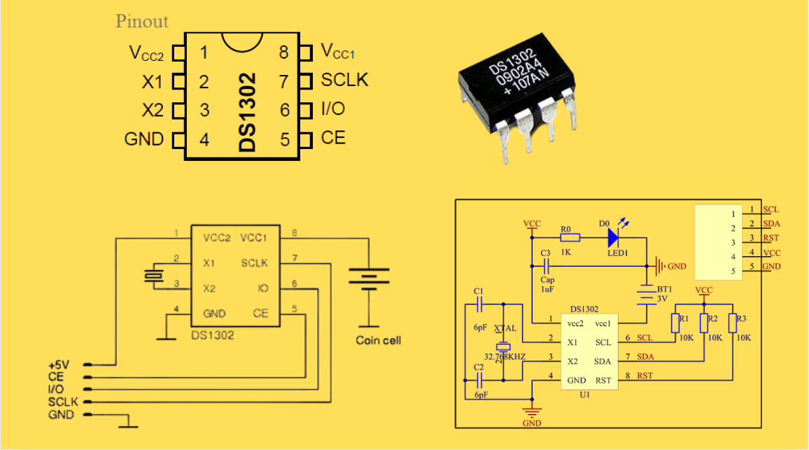
DS1302 RTC: Datasheet,Attributes,Features,Applications
As a low-power device widely used in electronic equipment, the DS1302 is centered on accurate real-time clock/calendar recording functions. It supports full-dimensional tracking of seconds, minutes, hours, days, weeks, months, and years, features automatic leap year compensation, and is compatible w...
-
2025 / 07 / 30
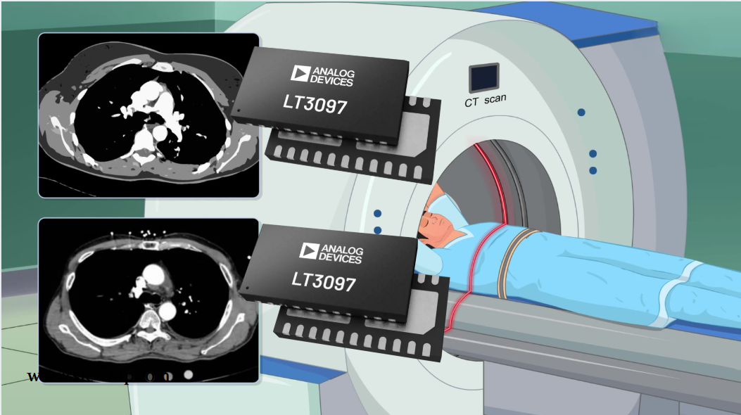
LT3097 Dual 500 mA, positive/negative, ultralow noise, ultrahigh PSRR low dropout linear regulator
The LT3097 is a dual, positive and negative, high-performance, low-dropout linear regulator featuring Analog Devices, Inc., ultralow noise and ultra-high power supply rejection ratio (PSRR) architecture for powering noise-sensitive applications. Each regulator delivers up to 500 mA with a typical 26...
-
2025 / 07 / 28
What is a Digital Integrated Circuit?
In the fast - paced world of modern electronics, digital integrated circuits (ICs) are the unsung heroes that power everything from our smartphones and laptops to complex supercomputers and industrial control systems. But what exactly is a digital integrated circuit?...
-
2025 / 07 / 25
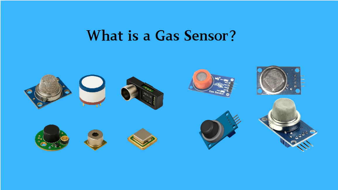
What is a Gas Sensor?
A gas sensor is a device that can convert information such as the composition and concentration of gas into electrical signals recognizable by electronic equipment. It is like the "olfactory organ" of an electronic system, capable of acutely detecting the presence of specific gases in the environmen...
-
2025 / 07 / 24
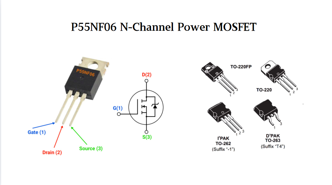
P55NF06 N-Channel Power MOSFET: Everything You Need To Know
In the vast landscape of semiconductor devices, MOSFETs (Metal - Oxide - Semiconductor Field - Effect Transistors) play a pivotal role, especially in power electronics. Among the numerous MOSFET models available, the P55NF06 stands out for its unique combination of features, making it suitable for a...
-
2025 / 07 / 23
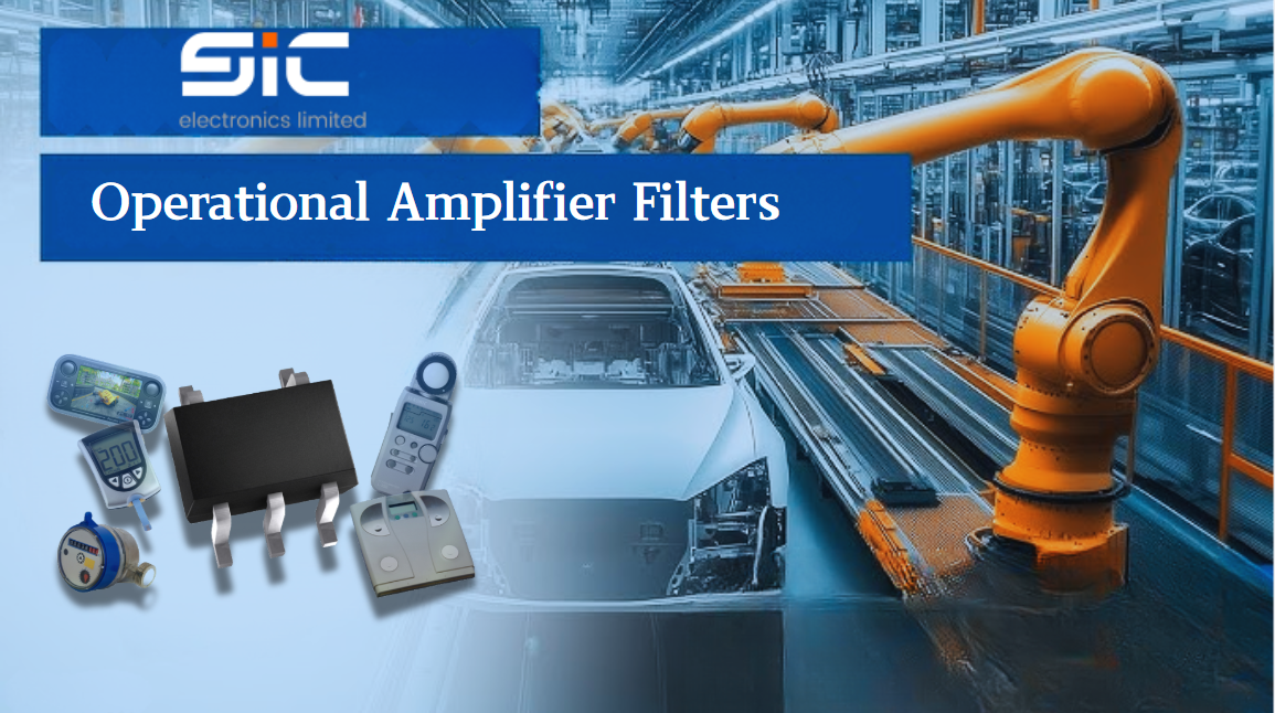
Operational Amplifier Filters: A Comprehensive Analysis from Fundamentals to Applications
In electronic systems, the purity and accuracy of signals directly determine the performance of devices. Electronic filters composed of operational amplifiers (op-amps) have become a "bridge" connecting original signals and valid information, thanks to their ability to precisely filter signal freque...
-
2025 / 07 / 19
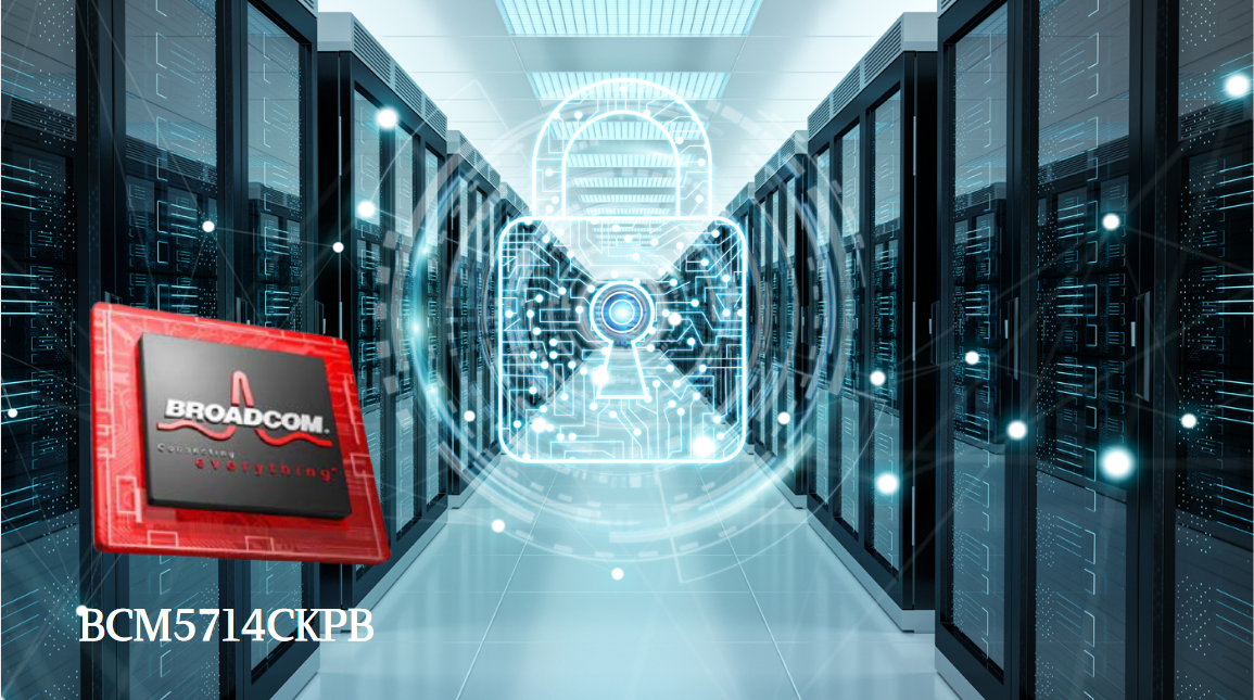
Broadcom BCM5714CKPB: Featrues,Applications,Datasheet And Advantages
When it comes to reliable, high-performance network connectivity in enterprise and industrial systems, the Broadcom BCM5714CKPB stands as a standout solution. This dual-port Gigabit Ethernet controller, developed by Broadcom—a leader in semiconductor innovation—combines robust features, versatile co...
-
2025 / 07 / 15
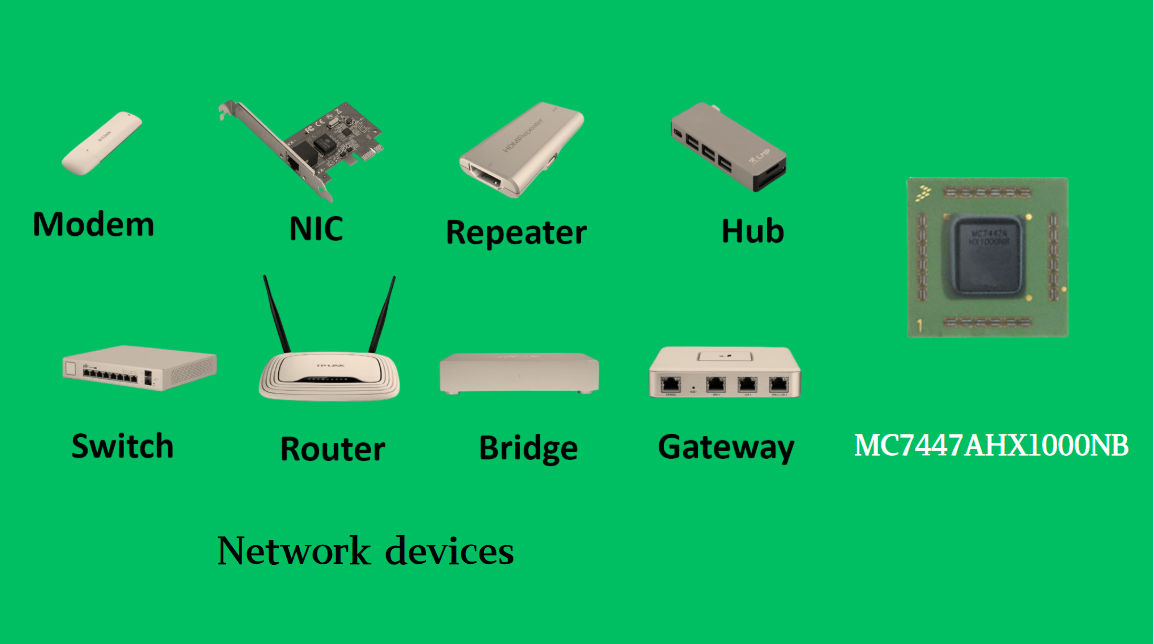
MC7447AHX1000NB: Technical Analysis and Applications of a High-Performance PowerPC Architecture Proc
In the field of embedded computing and network systems, the performance, energy efficiency, and compatibility of processors are often crucial to the success of a design. The MC7447AHX1000NB launched by NXP (formerly Freescale), as an important member of the MPC7447A series, has become an ideal choic...
-
2025 / 07 / 14
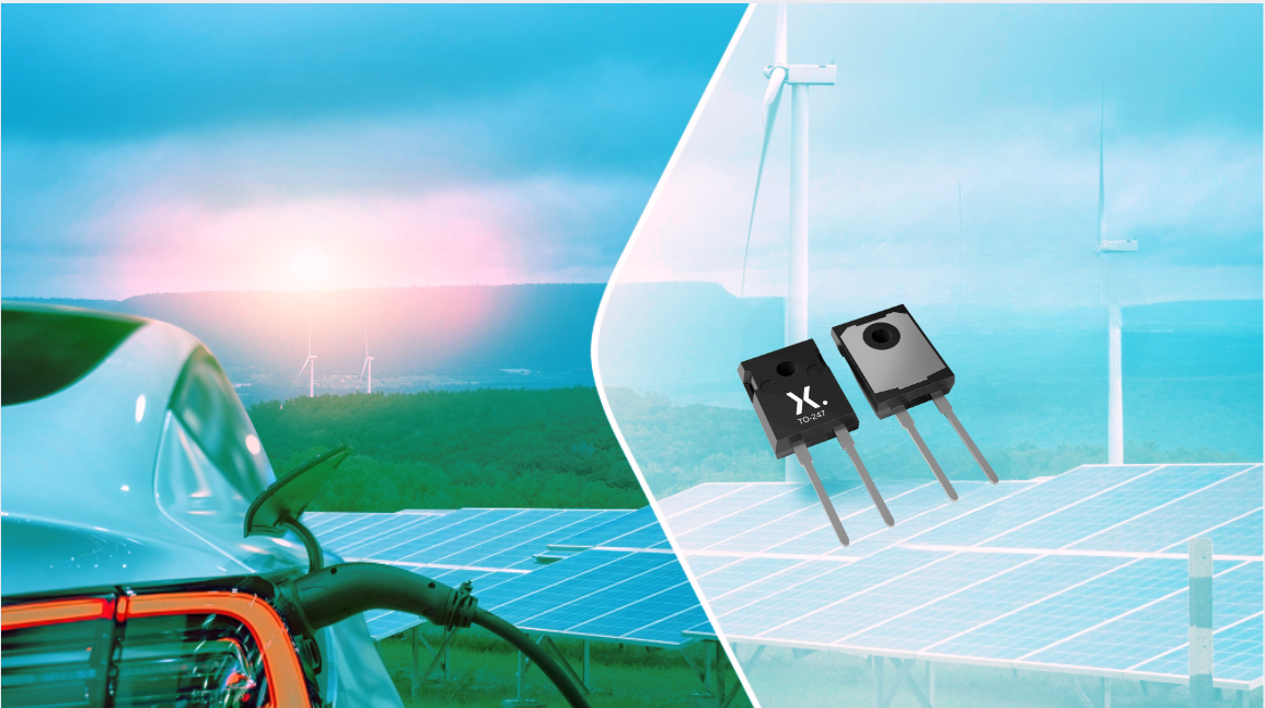
Nexperia Unveils New 1200V/20A SiC Schottky Diodes to Empower Efficient Industrial Power Innovations
Nexperia recently announced the addition of two new 1200V, 20A silicon carbide (SiC) Schottky diodes—PSC20120J and PSC20120L—to its power electronics portfolio, further expanding its product landscape in high-performance semiconductors. Specifically designed to address the increasingly stringent dem...
-
2025 / 07 / 09
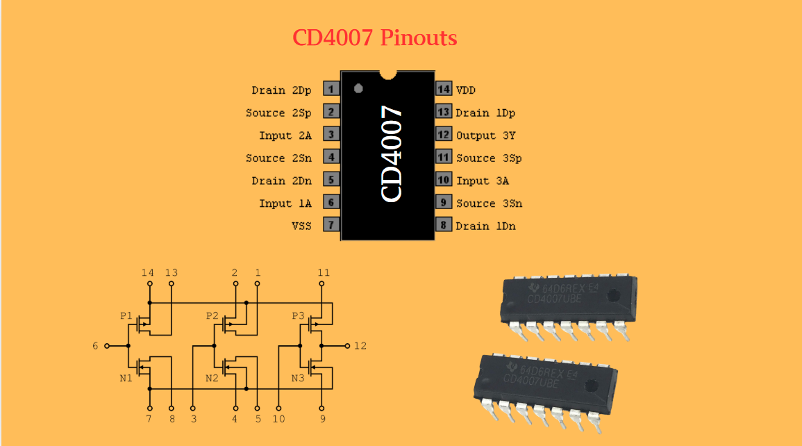
CD4007: A Comprehensive Analysis of a Multifunctional CMOS Integrated Circuit
In the field of modern electronic technology, CMOS (Complementary Metal-Oxide-Semiconductor) integrated circuits have become core components in digital and analog circuit design due to their low power consumption, high integration, and excellent compatibility. As a classic CMOS device, the CD4007 oc...

2000+
Daily average RFQ Volume

30,000,000
Standard Product Unit

2800+
Worldwide Manufacturers

15,000 m2
In-stock Warehouse
 Wishlist (0 Items)