

- RFQ
- BOM
-
Contact Us
Tel: +86-0755-83501315
Email: sales@sic-components.com


- Chinese
- English
- French
- German
- Portuguese
- Spanish
- Russian
- Japanese
- Korean
- Arabic
- Irish
- Greek
- Turkish
- Italian
- Danish
- Romanian
- Indonesian
- Czech
- Afrikaans
- Swedish
- Polish
- Basque
- Catalan
- Esperanto
- Hindi
- Lao
- Albanian
- Amharic
- Armenian
- Azerbaijani
- Belarusian
- Bengali
- Bosnian
- Bulgarian
- Cebuano
- Chichewa
- Corsican
- Croatian
- Dutch
- Estonian
- Filipino
- Finnish
- Frisian
- Galician
- Georgian
- Gujarati
- Haitian
- Hausa
- Hawaiian
- Hebrew
- Hmong
- Hungarian
- Icelandic
- Igbo
- Javanese
- Kannada
- Kazakh
- Khmer
- Kurdish
- Kyrgyz
- Latin
- Latvian
- Lithuanian
- Luxembou..
- Macedonian
- Malagasy
- Malay
- Malayalam
- Maltese
- Maori
- Marathi
- Mongolian
- Burmese
- Nepali
- Norwegian
- Pashto
- Persian
- Punjabi
- Serbian
- Sesotho
- Sinhala
- Slovak
- Slovenian
- Somali
- Samoan
- Scots Gaelic
- Shona
- Sindhi
- Sundanese
- Swahili
- Tajik
- Tamil
- Telugu
- Thai
- Ukrainian
- Urdu
- Uzbek
- Vietnamese
- Welsh
- Xhosa
- Yiddish
- Yoruba
- Zulu
- Kinyarwanda
- Tatar
- Oriya
- Turkmen
- Uyghur
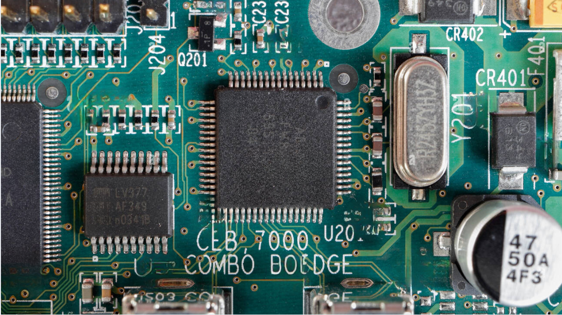
What is a Printed Circuit Board (PCB)? : A Comprehensive Guide
Printed Circuit Boards (PCBs) (https://www.sic-components.com/category-all) are the backbone of modern electronic devices. They serve as the physical platform that connects and enables the functionality of various electronic components, allowing for the seamless operation of everything from simple consumer electronics to complex industrial and aerospace systems.
1. What is a Printed Circuit Board (PCB)? https://www.sic-components.com/category-all
A Printed Circuit Board (PCB) is a thin, flat board made of insulating material, usually fiberglass, on which electronic components are mounted and electrically connected. It serves as the backbone of electronic devices, providing a physical structure for the components and enabling the transmission of electrical signals between them. PCBs are composed of several layers, including a substrate layer that provides mechanical support, conductive layers made of copper that form the electrical circuits, and insulating layers that separate the conductive layers to prevent short - circuits. The conductive layers are etched with intricate patterns of tracks and pads, which are designed to connect the various components in a specific way according to the circuit design. Components such as resistors, capacitors, integrated circuits, and connectors are mounted on the PCB through various methods, such as soldering. The PCB allows for the precise placement and interconnection of these components, ensuring the proper functioning of the electronic device. A PCB is an essential component in modern electronics, enabling the miniaturization, reliability, and mass - production of electronic devices by providing a standardized and efficient way to connect and organize electronic components.
2. PCBs Past and Present
The Past of Printed Circuit Boards (PCBs)
The origins of printed circuit boards can be traced back to the early 20th century. In the beginning, electronics were assembled using a rather rudimentary approach. Wires were used to connect individual components, and these components were mounted on a simple substrate. One of the earliest substrates was bakelite, a type of early plastic material.
During the 1930s and 1940s, as electronics became more complex and the demand for more compact and reliable circuits grew, the concept of the printed circuit board started to take shape. The first PCBs were relatively simple single-sided boards. Copper foil was bonded to a insulating base material, and the unwanted copper was etched away to create the conductive traces that connected the components. This was a significant improvement over the previous method of using individual wires, as it reduced the complexity of wiring and made the circuits more reliable.
In the post-World War II era, the development of printed circuit technology accelerated. The advent of transistors in the late 1940s and their increasing use in electronic circuits led to a further push for more efficient and compact circuit designs. Double-sided PCBs began to emerge, which allowed for more components to be packed onto the board and more complex circuit topologies to be realized. Through-hole technology (THT) became the standard method for mounting components on PCBs. Components had leads that were inserted through holes in the board and soldered on the other side, providing a secure mechanical and electrical connection.
As the electronics industry continued to grow in the 1960s and 1970s, the demand for even more sophisticated PCBs increased. Multilayer PCBs were developed, which consisted of multiple layers of conductive traces separated by insulating layers. This allowed for a much higher density of components and connections, enabling the creation of more powerful and complex electronic systems, such as mainframe computers and early minicomputers.
The Present of Printed Circuit Boards
Today, printed circuit boards have become an integral part of almost every electronic device. The technology has advanced significantly, driven by the ever-increasing demand for smaller, faster, and more powerful electronics.
Surface mount technology (SMT) has largely replaced through-hole technology as the dominant method for component mounting. SMT components are much smaller and can be directly soldered onto the surface of the PCB, allowing for a much higher component density. This has enabled the miniaturization of electronic devices, from smartphones and tablets to wearable devices.
High-density interconnect (HDI) PCBs are now widely used in modern electronics. These boards have extremely fine traces and vias, allowing for a much higher density of connections. HDI PCBs are essential for applications such as advanced microprocessors, high-speed data communication systems, and complex medical devices.
Flexible PCBs and rigid-flex PCBs have also become increasingly popular. Flexible PCBs are made from flexible materials such as polyimide and can be bent and flexed without damage. They are used in applications where space is limited and flexibility is required, such as in laptops, cameras, and some automotive components. Rigid-flex PCBs combine the features of both rigid and flexible PCBs, allowing for complex three-dimensional circuit layouts.
In addition, the design and manufacturing processes of PCBs have become highly automated. Computer-aided design (CAD) software is used to create the circuit designs, and computer-aided manufacturing (CAM) systems are used to fabricate the PCBs. This has increased the efficiency and accuracy of PCB production, while also reducing costs.
Furthermore, the materials used in PCBs have also evolved. Newer materials with better electrical and thermal properties are being developed, such as advanced laminates and high-performance dielectrics. These materials help to improve the performance and reliability of PCBs, especially in high-frequency and high-power applications.
Overall, the present state of printed circuit boards is characterized by high density, miniaturization, flexibility, and automation, enabling the creation of the advanced electronic devices that we rely on in our daily lives.
3. Types of PCBs https://www.sic-components.com/category-all
Printed Circuit Boards (PCBs) come in various types, each tailored to specific requirements and applications. Here is an in - depth look at the different types of PCBs:
3.1 Single - Sided PCBs
Structure and Design: As the name implies, single - sided PCBs have conductive traces on only one side of the board. The other side is usually a plain, non - conductive surface. They are the simplest type of PCB, with a single layer of copper etched to form the electrical pathways that connect components. The components are mounted on the side with the traces, and soldering is done on the same side.
Advantages:
Cost - effective: They are relatively inexpensive to manufacture because of their simple design and fewer manufacturing steps. The reduced complexity means lower material and production costs, making them an ideal choice for low - cost, large - scale production of simple electronic devices.
Easy to fabricate: The manufacturing process is straightforward, which also contributes to their affordability. This simplicity makes them accessible for hobbyists and small - scale projects where advanced features are not required.
Disadvantages:
Limited Component Density: Since all components and traces must be on one side, the number of components that can be placed on the board is limited. This restricts the complexity of the circuits that can be designed.
Complex Wiring Challenges: As the circuit becomes more complex, routing the traces without creating short - circuits or long, convoluted paths can be extremely difficult.
Applications: Commonly used in basic consumer electronics like calculators, simple toys, some LED lighting fixtures, and basic power adapters where the circuit design is not overly complex.
3.2 Double - Sided PCBs
Structure and Design: Double - sided PCBs feature conductive traces on both the top and bottom surfaces of the board. Components can be mounted on either or both sides, and electrical connections between the two sides are made through vias. Vias are small holes that are filled or plated with a conductive material, allowing signals to pass from one side of the board to the other.
Advantages:
Increased Component Density: With the ability to place components and traces on two sides, double - sided PCBs can accommodate more components and a more complex circuit design compared to single - sided PCBs. This makes them suitable for a wider range of applications.
Improved Signal Routing: The additional side provides more space for routing traces, reducing the likelihood of overly long or convoluted wiring. This can lead to better signal integrity and performance.
Disadvantages:
Higher Cost: The manufacturing process is more complex than that of single - sided PCBs, as it requires additional steps to create and connect the traces on the second side. This complexity results in higher production costs.
Assembly Complexity: Mounting components on both sides can make the assembly process more challenging and time - consuming, especially if manual assembly is involved.
Applications: Widely used in devices such as mobile phones, routers, modems, digital cameras, and many other consumer electronics where a more compact and feature - rich design is needed.
3.3 Multilayer PCBs
Structure and Design: Multilayer PCBs consist of three or more layers of conductive traces, separated by insulating layers. In addition to signal layers, they often include dedicated power and ground planes. The layers are laminated together under high pressure and temperature to form a single, rigid board. Vias are used to connect the different layers, allowing for complex interconnections between components.
Advantages:
High Component Density and Complexity: They can handle a large number of components and extremely complex circuit designs. The multiple layers provide ample space for routing traces, power distribution, and signal isolation, enabling the creation of high - performance electronic systems.
Improved Signal Integrity: The presence of dedicated power and ground planes helps to reduce electromagnetic interference (EMI) and improve signal integrity. This is crucial for high - speed digital circuits and applications where signal quality is of utmost importance.
Compact Size: By stacking the layers, multilayer PCBs can achieve a more compact form factor compared to using multiple single or double - sided PCBs, which is beneficial for miniaturized electronic devices.
Disadvantages:
High Cost: The manufacturing process is highly complex and requires precise control over multiple steps, including layer alignment, lamination, and via formation. This complexity leads to significantly higher production costs.
Longer Production Time: Due to the multiple layers and intricate manufacturing steps, the production time for multilayer PCBs is longer compared to single or double - sided PCBs.
Applications: Used in high - end electronics such as computer motherboards, graphics cards, servers, advanced medical equipment (e.g., MRI machines), aerospace avionics systems, and military electronics where high performance, reliability, and compactness are essential.
3.4 Flexible PCBs
Structure and Design: Flexible PCBs are made from a flexible substrate material, typically polyimide or polyester. The conductive traces are etched onto this flexible material, allowing the board to bend, fold, or twist without damage. Components can be mounted on the flexible board using surface - mount technology. Some flexible PCBs may also include stiffeners in certain areas to provide support for components or to facilitate connection to other parts of the device.
Advantages:
Space - Saving and Compact Design: Their flexibility allows them to be routed in tight spaces and around obstacles, enabling more creative and compact product designs. This is especially useful in applications where traditional rigid PCBs would be too bulky or inflexible.
Durability in Dynamic Environments: They can withstand repeated bending and flexing, making them suitable for applications where the PCB may be subject to movement or vibration, such as in wearable devices, automotive interiors, and some portable electronics.
Disadvantages:
Higher Cost: The materials used in flexible PCBs, as well as the more specialized manufacturing processes, make them more expensive than rigid PCBs.
Assembly Challenges: Mounting components on flexible PCBs can be more difficult due to the lack of rigidity, and special handling and assembly techniques are often required.
Applications: Found in wearable devices like smartwatches and fitness trackers, laptop hinges (for connecting the display to the main body), automotive dashboard displays, and some medical devices where a flexible form factor is necessary.
3.5 Rigid - Flex PCBs
Structure and Design: Rigid - flex PCBs combine the features of both rigid and flexible PCBs. They consist of one or more rigid sections connected by flexible sections. The rigid sections are used to mount and support components that require a stable platform, while the flexible sections allow for movement, bending, or folding of the board. These PCBs are often used in complex three - dimensional layouts where a combination of rigidity and flexibility is needed.
Advantages:
Versatile Design: They offer the best of both worlds, allowing for the creation of highly customized and complex designs that can fit into irregular spaces and accommodate moving parts.
Reduced Assembly Time and Cost: By integrating multiple PCBs into a single rigid - flex unit, the number of individual boards and connectors can be reduced, potentially saving on assembly time and costs.
Enhanced Reliability: Since there are fewer interconnections between separate boards, the risk of connection failures is reduced, leading to increased overall system reliability.
Disadvantages:
Complex Design and Manufacturing: Designing and manufacturing rigid - flex PCBs require advanced skills and specialized equipment. The combination of rigid and flexible sections makes the process more challenging, increasing the likelihood of errors during production.
Higher Cost: Due to the complexity of the design and manufacturing, as well as the use of specialized materials, rigid - flex PCBs are generally more expensive than traditional rigid or flexible PCBs.
Applications: Used in aerospace applications (e.g., satellite communication systems), medical devices (such as endoscopic equipment), and some high - end consumer electronics where a complex, space - efficient, and reliable design is required.
3.6 Metal - Core PCBs
Structure and Design: Metal - core PCBs have a metal substrate, usually aluminum, as the base layer instead of the traditional non - conductive material. The metal core provides excellent thermal conductivity, allowing for efficient heat dissipation. A thin layer of dielectric material is placed on top of the metal core, followed by the copper traces and components.
Advantages:
Superior Thermal Management: The metal core effectively conducts heat away from the components, preventing overheating and improving the reliability and lifespan of the electronic device. This is crucial for high - power applications where heat generation is significant.
Mechanical Strength: The metal substrate provides additional mechanical strength and rigidity to the PCB, making it more resistant to physical damage.
Disadvantages:
Higher Cost: The use of metal materials and the specialized manufacturing process to bond the dielectric and copper layers to the metal core increase the production cost.
Design Limitations: The metal core can pose challenges in terms of electrical isolation and signal routing, requiring careful design considerations to avoid interference and ensure proper functionality.
Applications: Commonly used in high - power lighting applications (e.g., LED streetlights, high - bay lights), automotive engine control units, power supplies, and other applications where efficient heat dissipation is essential.
3.7 Ceramic PCBs
Structure and Design: Ceramic PCBs are made from ceramic materials, such as alumina or aluminum nitride, which offer excellent electrical insulation and high thermal conductivity. The conductive traces are typically made of metals like copper or gold, which are bonded or printed onto the ceramic substrate.
Advantages:
High Thermal Conductivity: Ceramic materials can dissipate heat much more efficiently than traditional PCB substrates, making them suitable for high - power and high - temperature applications.
Excellent Electrical Properties: They have high dielectric strength, low dielectric loss, and good electrical insulation, which results in improved signal integrity and reduced interference, especially at high frequencies.
Chemical and Thermal Stability: Ceramic PCBs are highly resistant to chemicals, moisture, and thermal shock, making them reliable in harsh environments.
Disadvantages:
Brittle and Fragile: Ceramic materials are brittle, which makes the PCBs more prone to cracking or breaking during handling, assembly, or in the presence of mechanical stress.
High Cost: The manufacturing process of ceramic PCBs is complex and requires specialized equipment and techniques, leading to higher production costs compared to traditional PCBs.
Applications: Used in high - frequency applications (e.g., microwave and radio - frequency circuits), power electronics in harsh environments (such as aerospace and military applications), and some medical devices where reliability and high - performance are critical.
4. Who is Involved in Printed Circuit Board Design? https://www.sic-components.com/category-all
Electrical Engineers: They are responsible for designing the electrical circuit, determining the component placement, and ensuring the proper functioning of the board. They use their knowledge of electronics and circuit theory to create a design that meets the specific requirements of the device.
PCB Design Engineers: These professionals take the electrical design from the engineers and translate it into a physical layout on the PCB. They consider factors such as signal integrity, power distribution, and thermal management to ensure the board operates reliably. They also work with the manufacturing team to ensure the design is manufacturable.
Mechanical Engineers: They are involved in the overall design of the device that houses the PCB. They ensure that the PCB fits properly within the enclosure, taking into account factors such as size, shape, and mounting points. They also consider the mechanical stresses that the board may experience during operation and design accordingly.
5. The Process of Printed Circuit Board Design https://www.sic-components.com/category-all
5.1 Requirements Gathering
The first crucial step in printed circuit board (PCB) design is gathering requirements. Engineers need to understand the intended function of the electronic device that the PCB will serve. This includes determining the types of components that will be used, such as microcontrollers, integrated circuits, resistors, capacitors, and connectors. They also consider factors like the power requirements of the circuit, the operating voltage and current levels, and the expected performance in terms of speed, accuracy, and signal integrity.
Moreover, physical constraints play a significant role. The size and shape of the enclosure in which the PCB will be installed must be known. This helps in deciding the overall dimensions of the PCB. Environmental factors, such as temperature, humidity, and vibration levels that the device will be exposed to, also influence the design requirements. For example, in automotive or aerospace applications, the PCB needs to be able to withstand extreme temperatures and vibrations, which impacts the choice of materials and the robustness of the design.
5.2 Schematic Design
Once the requirements are clear, the next stage is schematic design. Using electronic design automation (EDA) software, engineers create a graphical representation of the electrical circuit. In this process, they place symbols for each component on the schematic sheet and connect them using wires or nets to represent the electrical connections.
Each component symbol has specific pins that correspond to its electrical terminals. For instance, a microcontroller symbol will have pins for power supply, data input/output, and control signals. By connecting these pins appropriately, the engineer defines how the components will interact with each other to perform the desired functions. During schematic design, it's essential to follow electrical design rules and best practices to ensure the circuit's functionality and reliability. This includes proper grounding, power distribution, and signal routing considerations at a conceptual level.
After creating the basic schematic, engineers often perform circuit simulations. Tools like SPICE (Simulation Program with Integrated Circuit Emphasis) are used to test the electrical behavior of the circuit. Simulations can predict how the circuit will respond to different input signals, check for potential issues such as signal reflections, crosstalk, and power supply noise, and verify that the components are operating within their specified parameters. Based on the simulation results, the schematic may be refined and adjusted as needed.
5.3 Library Part Creation or Selection
Simultaneously with or after schematic design, appropriate library parts for each component are either created or selected from existing libraries. EDA software relies on component libraries that contain information about each component's electrical characteristics, physical footprint, and 3D model (if available).
For standard off - the - shelf components, many EDA tools come with extensive libraries. However, for custom - designed components or those with unique packaging, engineers need to create new library parts. This involves defining the component's schematic symbol, footprint (the physical layout of the pads on the PCB where the component will be mounted), and any associated simulation models. Accurate library parts are crucial for both the schematic design and the subsequent PCB layout stages, as they ensure that the component will fit correctly on the board and function as expected.
5.4 PCB Layout Design
Component Placement
With the schematic and library parts ready, the focus shifts to the PCB layout design. The first step in layout is component placement. The engineer imports the netlist from the schematic, which contains information about the electrical connections between components. Using the EDA software, they then position the component footprints on the PCB within the defined board outline.
Component placement is a critical decision - making process. Components need to be arranged in a way that optimizes signal routing, minimizes electromagnetic interference (EMI), and considers thermal management. For example, heat - generating components like power transistors or microprocessors should be placed in areas with good ventilation or near heat sinks. High - speed components and signals should be grouped together and routed with minimal length and interference. Additionally, mechanical constraints, such as the location of mounting holes, connectors, and other external interfaces, also influence component placement. The goal is to create a layout that is both electrically functional and manufacturable.
Routing
After component placement, the next step is routing the traces that connect the components. Traces are the conductive pathways on the PCB, usually made of copper, that carry electrical signals between component pins. EDA software provides various routing tools, including automatic routing algorithms and manual routing capabilities.
During routing, several factors need to be considered. Signal integrity is of utmost importance, especially for high - speed signals. Traces need to be routed with proper impedance control to prevent signal reflections and distortion. To achieve this, the width, length, and spacing of the traces are carefully designed according to the signal requirements. Crosstalk between adjacent traces, which can cause unwanted interference, must also be minimized. This can be done by increasing the spacing between traces, using shielding techniques, or proper trace routing strategies.
Power traces require special attention as well. They need to be wide enough to handle the required current without excessive voltage drop and should be routed in a way that provides a stable power supply to all components. Ground traces and planes are also crucial for providing a low - impedance return path for the current and reducing EMI.
Plane Definition
In addition to routing individual traces, power and ground planes are defined in the PCB layout. Power planes are large areas of copper that distribute power to the components, while ground planes provide a common electrical reference. These planes are typically created on separate layers of the PCB.
Power planes are often split into different regions to supply power to different parts of the circuit with specific voltage requirements. For example, a PCB may have separate power planes for analog and digital circuits to prevent interference between them. Ground planes help in reducing electromagnetic radiation, improving signal integrity, and providing a stable electrical environment. By carefully defining and routing the power and ground planes, engineers can ensure efficient power distribution and minimize noise in the circuit.
5.5 Design Rules Checking (DRC)
Once the routing and plane definition are complete, a design rules check (DRC) is performed using the EDA software. DRC verifies that the PCB layout complies with a set of predefined design rules. These rules cover aspects such as minimum trace width, minimum clearance between traces, via size and spacing, and component placement constraints.
The software scans the entire layout and flags any violations of these rules. For example, if a trace width is too narrow for the expected current, or if two traces are too close together, it will be reported as a DRC violation. Addressing these violations is essential to ensure the manufacturability and functionality of the PCB. Engineers need to go back and modify the layout, such as adjusting trace widths, rerouting traces, or changing component positions, until all DRC violations are resolved.
5.6 Gerber File Generation and Documentation
After passing the DRC, the final step in the PCB design process is generating Gerber files. Gerber files are the standard format used to communicate the PCB design to the manufacturer. They contain detailed information about the copper layers, solder mask, silkscreen, drill holes, and other aspects of the PCB.
In addition to Gerber files, other documentation such as assembly drawings, bill of materials (BOM), and test specifications may also be prepared. The assembly drawings provide instructions for mounting the components on the PCB, while the BOM lists all the components required for the assembly, including their part numbers, descriptions, and quantities. The test specifications define the procedures and criteria for testing the completed PCB to ensure it meets the design requirements.
Once these files and documents are ready, they are sent to the PCB manufacturer for fabrication and assembly. The design process may also involve collaboration with the manufacturer during this stage to address any questions or concerns regarding the design and ensure a smooth transition from design to production.
6. PCB Design Considerations https://www.sic-components.com/category-all
Signal Integrity: This is crucial for ensuring the accurate transmission of signals between components. Factors such as trace length, impedance matching, and crosstalk must be considered to prevent signal distortion and errors.
Power Distribution: The PCB must be designed to provide a stable and reliable power supply to the components. This involves proper placement of power rails, decoupling capacitors, and consideration of power loss and heat generation.
Thermal Management: As electronic components generate heat during operation, proper thermal management is essential to prevent overheating and ensure the reliability of the board. This can be achieved through the use of heat sinks, thermal vias, and proper component placement.
EMI/EMC: Electromagnetic interference (EMI) and electromagnetic compatibility (EMC) must be considered to prevent the PCB from interfering with other devices and to ensure that it is immune to external interference. This can be achieved through shielding, proper grounding, and careful layout of the components and traces.
7. Printed Circuit Board Layers
Signal Layers: These are the layers where the electrical traces that carry the signals between components are located. The number of signal layers depends on the complexity of the circuit and the available space on the board.
Power and Ground Layers: Dedicated layers are used for distributing power and providing a ground reference. These layers help to reduce noise and interference and ensure a stable power supply.
Dielectric Layers: These layers separate the conductive layers and provide insulation. They also affect the electrical characteristics of the board, such as the signal propagation speed and impedance.
Solder Mask Layer: This is a thin layer of insulating material that is applied over the copper traces to prevent solder from sticking to the wrong areas during the component mounting process. It also provides protection against corrosion and mechanical damage.
Silkscreen Layer: The silkscreen layer is used to print labels, markings, and component outlines on the board. This helps with the identification and assembly of the components.
8. Printed Circuit Board Components
Integrated Circuits (ICs): These are the most complex components on a PCB, containing multiple transistors, resistors, and other elements integrated into a single chip. They perform various functions such as signal processing, data storage, and control.
Resistors: They are used to limit the flow of current in a circuit and to set the voltage levels. They come in different values and power ratings.
Capacitors: Capacitors store and release electrical charge, and are used for filtering, coupling, and bypassing signals. They are available in different types, such as ceramic, electrolytic, and tantalum capacitors.
Inductors: Inductors are used to store energy in a magnetic field and are often used in power supply circuits and filters. They can be either discrete components or integrated into power inductors.
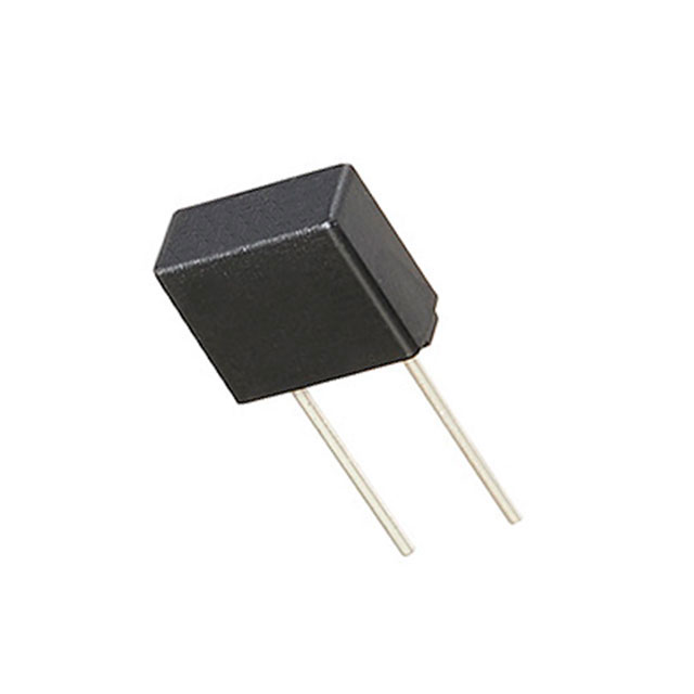
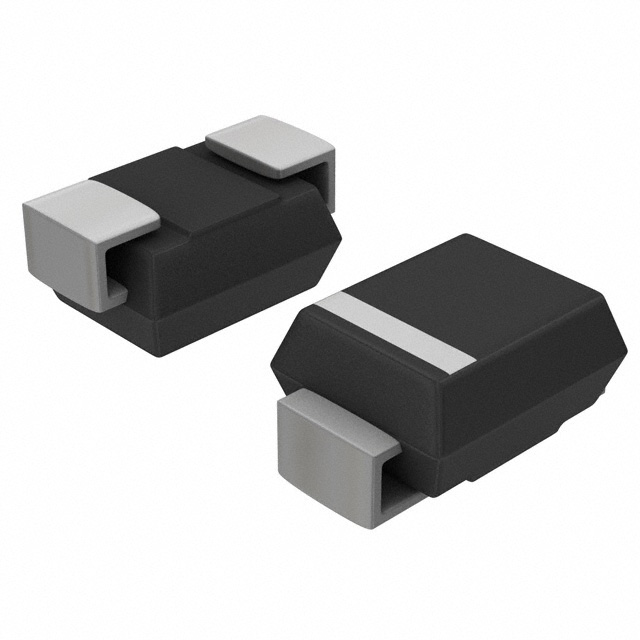
Diodes: Diodes allow current to flow in only one direction and are used for rectification, voltage regulation, and protection against reverse voltage.
Component Mounting
Surface - Mount Technology (SMT): This is the most common method of component mounting today. SMT components are mounted directly onto the surface of the PCB using solder paste and reflow soldering. This method allows for high - density packing of components and reduces the size and cost of the PCB.
Through - Hole Technology (THT): In THT, the components have leads that are inserted through holes in the PCB and soldered on the other side. This method is more suitable for larger components and those that require a more robust mechanical connection, such as power transformers and some connectors.
9. Where are Printed Circuit Boards Used? https://www.sic-components.com/category-all
Consumer Electronics: As mentioned earlier, PCBs are found in almost all consumer electronic devices, from smartphones and tablets to audio - visual equipment and home appliances. They enable the integration of various functions into a single device, providing users with convenient and powerful electronic products.
Industrial Applications: In the industrial sector, PCBs are used in automation systems, motor drives, programmable logic controllers (PLCs), and industrial computers. They help to improve the efficiency and reliability of industrial processes.
Medical Devices: The medical field relies on PCBs for a wide range of devices, including diagnostic equipment, treatment devices, and patient monitoring systems. The high reliability and precision of PCBs are crucial for ensuring the safety and effectiveness of these medical devices.
Aerospace and Defense: PCBs are used in avionics systems, radar systems, missile guidance systems, and communication equipment in the aerospace and defense industries. They must meet strict requirements for reliability, performance, and environmental resistance.
Automotive Industry: In cars, PCBs are used in engine control units (ECUs), infotainment systems, airbag control modules, and other electronic systems. They help to improve the performance, safety, and comfort of vehicles.
10. The Future of PCBs
Continued Miniaturization: With the increasing demand for smaller and more powerful electronic devices, PCBs will continue to be miniaturized. This will require the development of new manufacturing processes and materials to enable the production of even smaller and more complex PCBs.
Higher Performance: As the requirements for electronic devices become more demanding, PCBs will need to offer higher performance in terms of signal speed, power handling, and thermal management. This will drive the development of new materials and design techniques to meet these challenges.
Integration of New Technologies: The future of PCBs will see the integration of new technologies such as 3D printing, nanotechnology, and flexible electronics. These technologies will enable the development of more innovative and functional PCBs, opening up new applications in areas such as wearable electronics, biomedical devices, and the Internet of Things (IoT).
Sustainability: With increasing environmental concerns, there will be a growing focus on the sustainability of PCB manufacturing. This will involve the use of more environmentally friendly materials, the reduction of waste and energy consumption, and the development of recycling and disposal methods for PCBs.
In conclusion, printed circuit boards have come a long way since their inception and continue to play a vital role in the modern electronics industry. As technology continues to evolve, PCBs will also evolve to meet the changing needs of various applications, offering new opportunities for innovation and growth.
https://www.sic-components.com/category-all
Hot Products
View More-

TA45-ABFBS040C0-AZM01 SCHURTER Inc.
-
0001.2704.11 SCHURTER Inc.
-
IELK111-39531-1-V Sensata-Airpax
-
MAP4KE9.1AE3 Microchip Technology
-
IEGHF66-29977-2-V Sensata-Airpax
-

5KP170A Littelfuse Inc.
-
SZNS6A36AFT3G Littelfuse Inc.
-
CBP-10B Eaton - Bussmann Electrical Division
-
3500-F11-P10-A3-0.5A E-T-A
-
1301530171 Molex
-
TA45-ABFGT070C0-AZM10 SCHURTER Inc.
-
MMS-100H-26A Altech Corporation
Related Blogs
-
2025 / 08 / 01
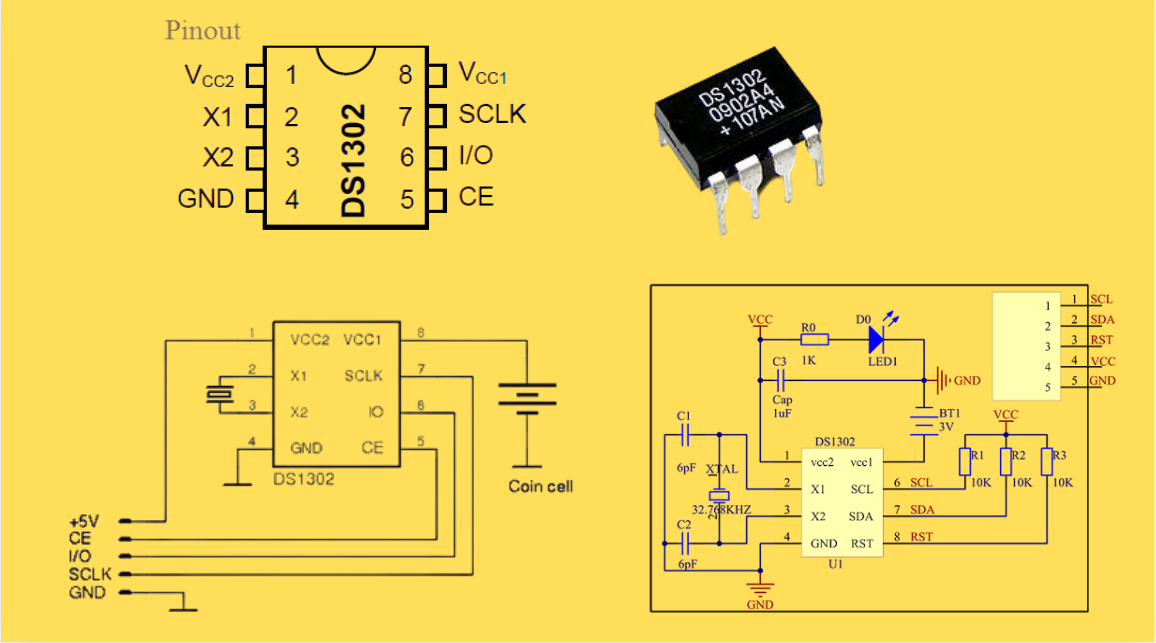
DS1302 RTC: Datasheet,Attributes,Features,Applications
As a low-power device widely used in electronic equipment, the DS1302 is centered on accurate real-time clock/calendar recording functions. It supports full-dimensional tracking of seconds, minutes, hours, days, weeks, months, and years, features automatic leap year compensation, and is compatible w...
-
2025 / 07 / 30
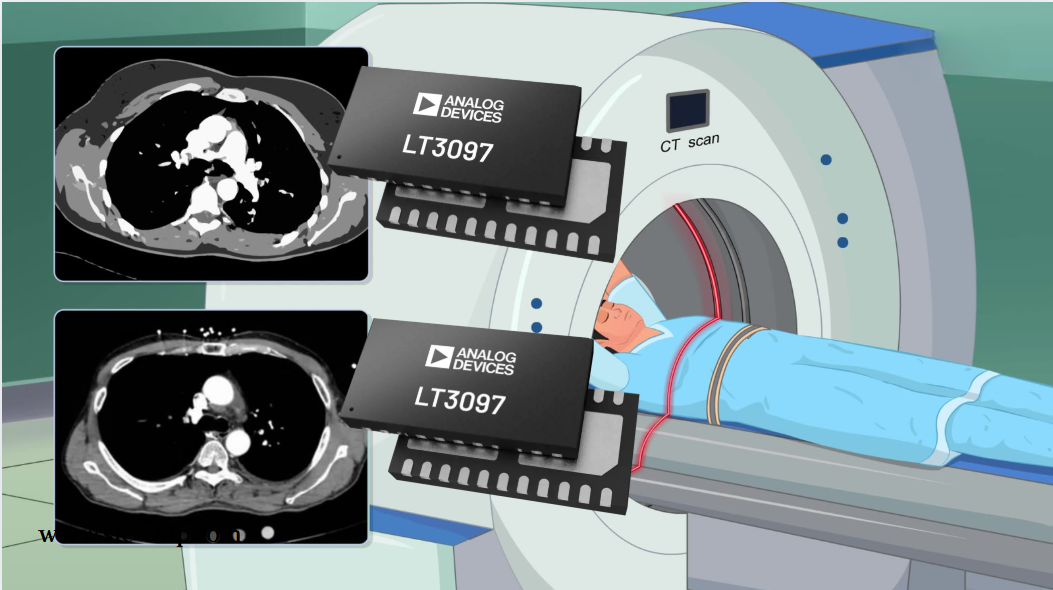
LT3097 Dual 500 mA, positive/negative, ultralow noise, ultrahigh PSRR low dropout linear regulator
The LT3097 is a dual, positive and negative, high-performance, low-dropout linear regulator featuring Analog Devices, Inc., ultralow noise and ultra-high power supply rejection ratio (PSRR) architecture for powering noise-sensitive applications. Each regulator delivers up to 500 mA with a typical 26...
-
2025 / 07 / 28
What is a Digital Integrated Circuit?
In the fast - paced world of modern electronics, digital integrated circuits (ICs) are the unsung heroes that power everything from our smartphones and laptops to complex supercomputers and industrial control systems. But what exactly is a digital integrated circuit?...
-
2025 / 07 / 25
What is a Gas Sensor?
A gas sensor is a device that can convert information such as the composition and concentration of gas into electrical signals recognizable by electronic equipment. It is like the "olfactory organ" of an electronic system, capable of acutely detecting the presence of specific gases in the environmen...
-
2025 / 07 / 24
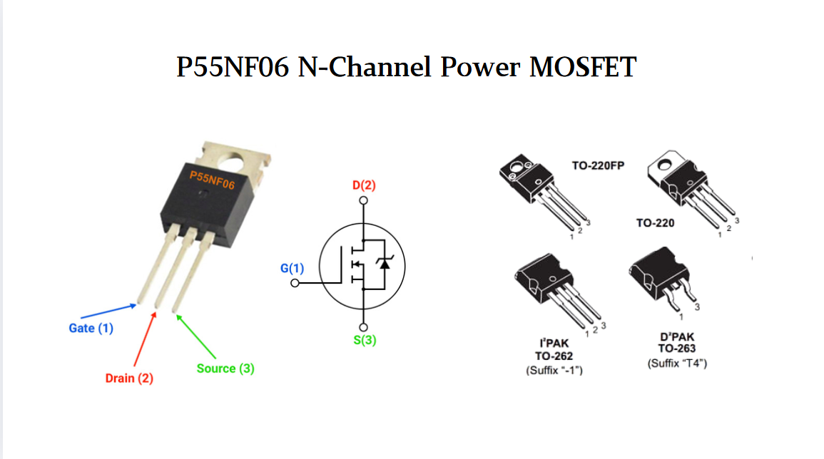
P55NF06 N-Channel Power MOSFET: Everything You Need To Know
In the vast landscape of semiconductor devices, MOSFETs (Metal - Oxide - Semiconductor Field - Effect Transistors) play a pivotal role, especially in power electronics. Among the numerous MOSFET models available, the P55NF06 stands out for its unique combination of features, making it suitable for a...
-
2025 / 07 / 23
Operational Amplifier Filters: A Comprehensive Analysis from Fundamentals to Applications
In electronic systems, the purity and accuracy of signals directly determine the performance of devices. Electronic filters composed of operational amplifiers (op-amps) have become a "bridge" connecting original signals and valid information, thanks to their ability to precisely filter signal freque...

-
2025 / 07 / 19
Broadcom BCM5714CKPB: Featrues,Applications,Datasheet And Advantages
When it comes to reliable, high-performance network connectivity in enterprise and industrial systems, the Broadcom BCM5714CKPB stands as a standout solution. This dual-port Gigabit Ethernet controller, developed by Broadcom—a leader in semiconductor innovation—combines robust features, versatile co...

-
2025 / 07 / 15
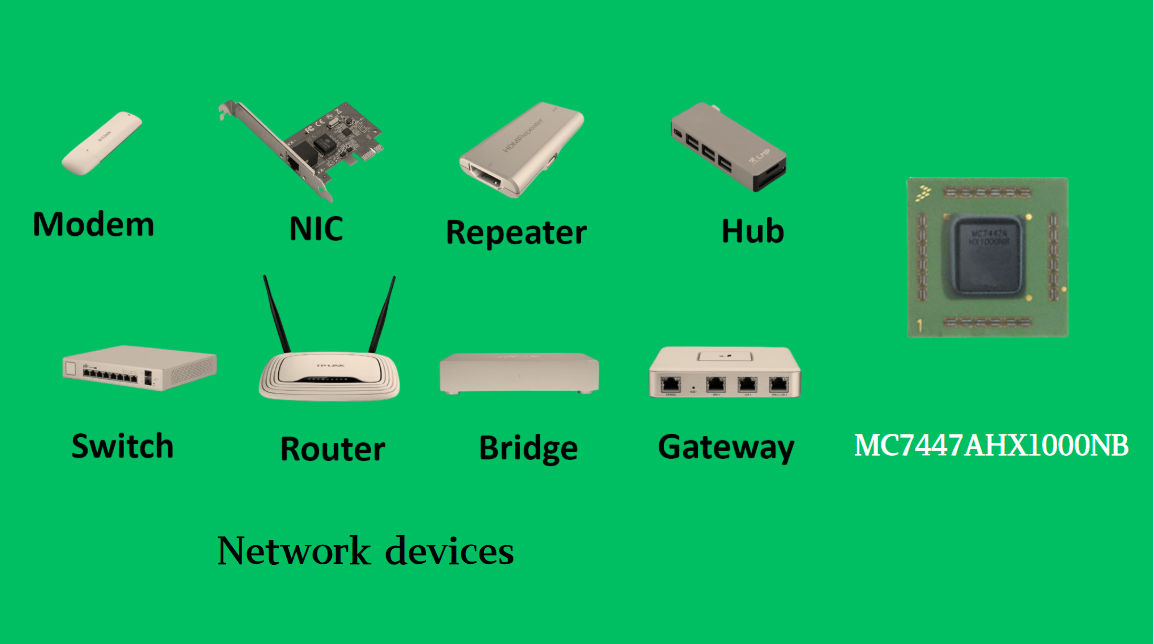
MC7447AHX1000NB: Technical Analysis and Applications of a High-Performance PowerPC Architecture Proc
In the field of embedded computing and network systems, the performance, energy efficiency, and compatibility of processors are often crucial to the success of a design. The MC7447AHX1000NB launched by NXP (formerly Freescale), as an important member of the MPC7447A series, has become an ideal choic...
-
2025 / 07 / 14
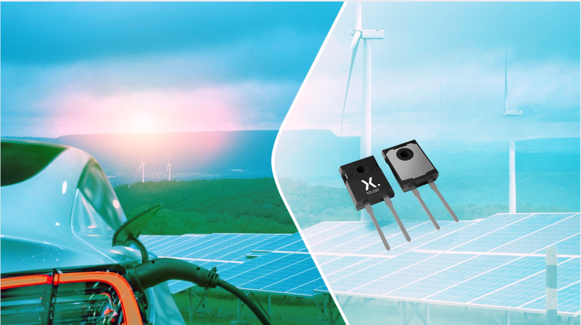
Nexperia Unveils New 1200V/20A SiC Schottky Diodes to Empower Efficient Industrial Power Innovations
Nexperia recently announced the addition of two new 1200V, 20A silicon carbide (SiC) Schottky diodes—PSC20120J and PSC20120L—to its power electronics portfolio, further expanding its product landscape in high-performance semiconductors. Specifically designed to address the increasingly stringent dem...
-
2025 / 07 / 09
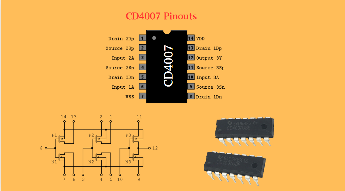
CD4007: A Comprehensive Analysis of a Multifunctional CMOS Integrated Circuit
In the field of modern electronic technology, CMOS (Complementary Metal-Oxide-Semiconductor) integrated circuits have become core components in digital and analog circuit design due to their low power consumption, high integration, and excellent compatibility. As a classic CMOS device, the CD4007 oc...

2000+
Daily average RFQ Volume

30,000,000
Standard Product Unit

2800+
Worldwide Manufacturers

15,000 m2
In-stock Warehouse
 Wishlist (0 Items)