

- RFQ
- BOM
-
Contact Us
Tel: +86-0755-83501315
Email: sales@sic-components.com


- Chinese
- English
- French
- German
- Portuguese
- Spanish
- Russian
- Japanese
- Korean
- Arabic
- Irish
- Greek
- Turkish
- Italian
- Danish
- Romanian
- Indonesian
- Czech
- Afrikaans
- Swedish
- Polish
- Basque
- Catalan
- Esperanto
- Hindi
- Lao
- Albanian
- Amharic
- Armenian
- Azerbaijani
- Belarusian
- Bengali
- Bosnian
- Bulgarian
- Cebuano
- Chichewa
- Corsican
- Croatian
- Dutch
- Estonian
- Filipino
- Finnish
- Frisian
- Galician
- Georgian
- Gujarati
- Haitian
- Hausa
- Hawaiian
- Hebrew
- Hmong
- Hungarian
- Icelandic
- Igbo
- Javanese
- Kannada
- Kazakh
- Khmer
- Kurdish
- Kyrgyz
- Latin
- Latvian
- Lithuanian
- Luxembou..
- Macedonian
- Malagasy
- Malay
- Malayalam
- Maltese
- Maori
- Marathi
- Mongolian
- Burmese
- Nepali
- Norwegian
- Pashto
- Persian
- Punjabi
- Serbian
- Sesotho
- Sinhala
- Slovak
- Slovenian
- Somali
- Samoan
- Scots Gaelic
- Shona
- Sindhi
- Sundanese
- Swahili
- Tajik
- Tamil
- Telugu
- Thai
- Ukrainian
- Urdu
- Uzbek
- Vietnamese
- Welsh
- Xhosa
- Yiddish
- Yoruba
- Zulu
- Kinyarwanda
- Tatar
- Oriya
- Turkmen
- Uyghur
Gallium nitride (GaN) power ICs
I. Technological Evolution: From Material Advantages to IC Integration
As a third-generation semiconductor material, gallium nitride (GaN) fundamentally breaks through the performance ceiling of silicon-based devices with its 3.4 eV wide bandgap, 3.3 MV/cm breakdown field strength, and 2000 cm²/V·s electron mobility. Compared with traditional silicon MOSFETs, GaN power ICs integrate HEMT (high electron mobility transistors) with driver and protection circuits through monolithic integration, achieving a leap forward with 70% lower switching losses and 3 times higher power density. For example, Navitas' GaNfast series uses All GaN™ process to integrate 650V e-mode HEMT with totem-pole drivers in a 5x6mm BGA package, reducing the switching loop inductance to below 1nH and supporting 2MHz high-frequency operation, shrinking 65W fast chargers to 1/3 the size of traditional silicon solutions.
Key technological milestones:
2010: EPC launches the first enhanced GaN FET (eGaN®), solving the normally-on challenge of depletion-mode devices.
2016: Mass production of integrated driver GaN power ICs initiates the fast charging revolution in consumer electronics.
2023: 8-inch GaN-on-Si wafer yield exceeds 90%, driving industrial application costs down by 60%.
II. Core Advantages: Reconstructing Power Electronics Design Paradigms
1. Electrical Performance Leap
Metric GaN Power IC (EPC2055) Silicon MOSFET (same power) Advantage
Switching Frequency 2MHz 50kHz ↑40x
RDS(on) 3.6mΩ 16mΩ ↓77.5%
Power Density 17W/cm³ 5W/cm³ ↑240%
Efficiency 94% 88% ↑6.8%
2. System-Level Advantage Realization
High-frequency dividends: 1MHz+ switching frequency reduces magnetic component volume by 80%. OPPO's 50W GaN charger eliminates electrolytic capacitors via 2MHz pulse ACF technology, achieving 12.8mm thickness.
Simplified thermal management: Although thermal conductivity (1.3W/cm·K) is slightly lower than silicon, reduced switching losses lower actual junction temperature by 50°C, enabling natural cooling for most scenarios.
Reliability enhancement: Integrated overcurrent/overtemperature protection responds in 33ns, 50% faster than discrete solutions. For example, a 200V GaN IC developed by the University of Toronto achieves 33ns overcurrent protection.
3. Cost-Efficiency Balance
2025 data shows 1200V GaN power ICs cost 80% of SiC while maintaining 3x faster switching speeds. In 65W fast charging, GaN solutions have 15% higher BOM costs than silicon, but energy efficiency savings offset the premium within 1.5 years.
III. Technical Architecture: Integration Innovation from Devices to Systems
1. Integration Hierarchy Analysis
Level 0-1 integration: Driver and level shifting. Representative product EPC2040 integrates 15V/0.745mΩ HEMT with 5V driver for Class-D audio amplification.
Level 2 integration: On-chip sensing. Infineon's GaN IC embeds current-sensing HEMT for full-cycle fault protection.
Level 3-4 integration: Full closed-loop control. A University of Toronto 400V-150V converter prototype integrates differential power processing algorithms to optimize battery pack energy distribution.
2. Key Process Breakthroughs
GaN-on-Si epitaxy: 8-inch wafers reduce defect density to 10^6/cm² via MOCVD, approaching SiC levels.
Gate engineering: AlGaN/GaN heterojunction increases threshold voltage from 1.7V to 2.5V, enhancing noise immunity by 30%.
3D packaging: Vicor ChiP technology vertically stacks GaN and planar transformers, achieving 1500W/in³ power density.
IV. Application Penetration: From Consumer Electronics to Energy Revolution
1. Consumer Electronics: Disrupting Fast Charging
The global GaN fast charging market will reach $1.2 billion by 2025, with 35% penetration. Anker's 747 charger uses GaN IC to achieve 240W power in 1/3 the size of equivalent silicon solutions. The deeper innovation is "pulse charging"—2MHz high-frequency pulses eliminate battery polarization, extending cycle life by 20%.
2. New Energy Vehicles: Core Enabler for 800V Platforms
In on-board chargers (OBCs), GaN power ICs with 100kHz full-bridge LLC topology reduce 6.6kW module volume by 40% and achieve 97% efficiency. Tesla Model Y's 11kW OBC uses TI's GaN solution, reducing weight by 2kg and charging speed by 30%. Yole predicts GaN will penetrate 28% of automotive charging modules by 2028.
3. Industrial & Energy: Efficiency Revolution in High-Voltage Scenarios
Data centers: Vicor ChiP technology provides 48V-to-12V power for AI servers with 1500W/in³ density, reducing cooling costs by 40%.
Photovoltaic inverters: 1200V GaN ICs support 1MHz switching, improving 10kW device efficiency by 10% and volume by 35%. The industrial GaN market grew 67% in 2024.
4. Aerospace & Defense: Extreme Environment Applications
EPC7002 radiation-hardened GaN ICs power satellite systems, withstanding 100kRad radiation and operating from -55°C to 125°C, enabling rapid deployment of low-Earth satellite constellations.
V. Challenges and Breakthroughs: Technical Bottlenecks and Strategies
1. Endogenous Technical Challenges
Logic integration limitations: Lack of PMOS causes RTL logic leakage 10x higher than CMOS. University of Toronto's GaN-on-SOI process reduces logic circuit area by 50% via trench isolation.
Thermal constraints: Micro-channel cooling is needed for >10kW scenarios, increasing costs by 15%. Solutions include copper substrate packaging (thermal resistance 0.5°C/W) and intelligent thermal management algorithms.
2. Ecosystem Pain Points
Design toolchain: Cadence and Navitas collaborate to launch GaN PDK with 200+ device models, shortening design cycles from 18 to 9 months.
Mass production economy: 8-inch GaN-on-Si wafer yield exceeds 90%, with 1200V device costs expected to match silicon by 2026.
VI. Future Trends: Paradigm Shift from High-Frequency to Intelligence
1. Device Structure Innovations
PMOS HEMT breakthroughs: AlGaN/GaN heterojunction PMOS is expected to achieve >2V threshold voltage by 2026, solving high-leakage logic circuit issues.
Ultra-high voltage devices: PI's 1700V InnoMux™-2 for energy storage converters will achieve 2000V breakthrough by 2027, covering rail transit auxiliary power.
2. Intelligence and System Integration
Digital PID control: STM32G4 MCUs collaborating with GaN ICs shortens load transient response to 50 microseconds, enabling AI algorithms for capacitor aging prediction.
Energy internet adaptation: GaN power ICs integrate MPPT algorithms, reducing photovoltaic inverter levelized cost of energy by 15% and enabling solar-storage-charging integration.
3. Packaging and Manufacturing Innovations
Heterogeneous integration: TSMC's CoWoS technology 3D-packages GaN ICs with silicon control chips, reducing 5G base station power supply volume by 1/4.
Cost control: GaN-on-silicon substrate costs will drop to 1/3 of SiC by 2025, driving full GaN adoption for <100W consumer electronics.
VII. Conclusion: Industrial Positioning and Value of GaN Power ICs
From 65W mobile chargers to 11kW vehicle chargers, GaN power ICs reshape power electronics with integration, high frequency, and intelligence. As 1700V devices break through high-voltage barriers and 8-inch mass production lowers thresholds, GaN is no longer just a "fast charging chip" but the cornerstone of the energy internet. With material process maturity and ecosystem perfection, this technological innovation starting in consumer electronics will eventually sweep through industrial, automotive, and energy sectors—just as transistors replaced vacuum tubes, the "beauty of integration" in GaN power ICs is defining the next golden decade of power semiconductors.
https://www.sic-components.com/category-all


Hot Products
View More-

DTS050400UDC-P5P-TK CUI Inc.
-
POE30S-1ATG-R Phihong USA
-
IMP4-1S0-1E0-1I0-1I0-4LF-00 Artesyn Embedded Power
-

CX10S-BBDHGH-P-A-DK00000 Advanced Energy
-
ME240A3251F01 SL Power Electronics Manufacture of Condor/Ault Brands
-
CX10S-AH0HDC-P-A-DK00000 Advanced Energy
-
CX10S-BAH0AA-P-A-DK00000 Advanced Energy
-
VI-RC3114-EYYV Vicor Corporation
-
MP4-74568 Vicor Corporation
-
NMP1K2-EHCKEE-05 MEAN WELL USA Inc.
-
CX10S-0CACCG-P-A-DK00000 Advanced Energy
-
VI-PU3N-EWY Vicor Corporation
Related Blogs
-
2025 / 07 / 25
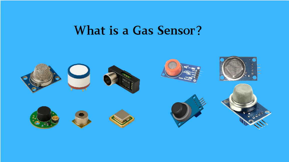
What is a Gas Sensor?
A gas sensor is a device that can convert information such as the composition and concentration of gas into electrical signals recognizable by electronic equipment. It is like the "olfactory organ" of an electronic system, capable of acutely detecting the presence of specific gases in the environmen...
-
2025 / 07 / 24
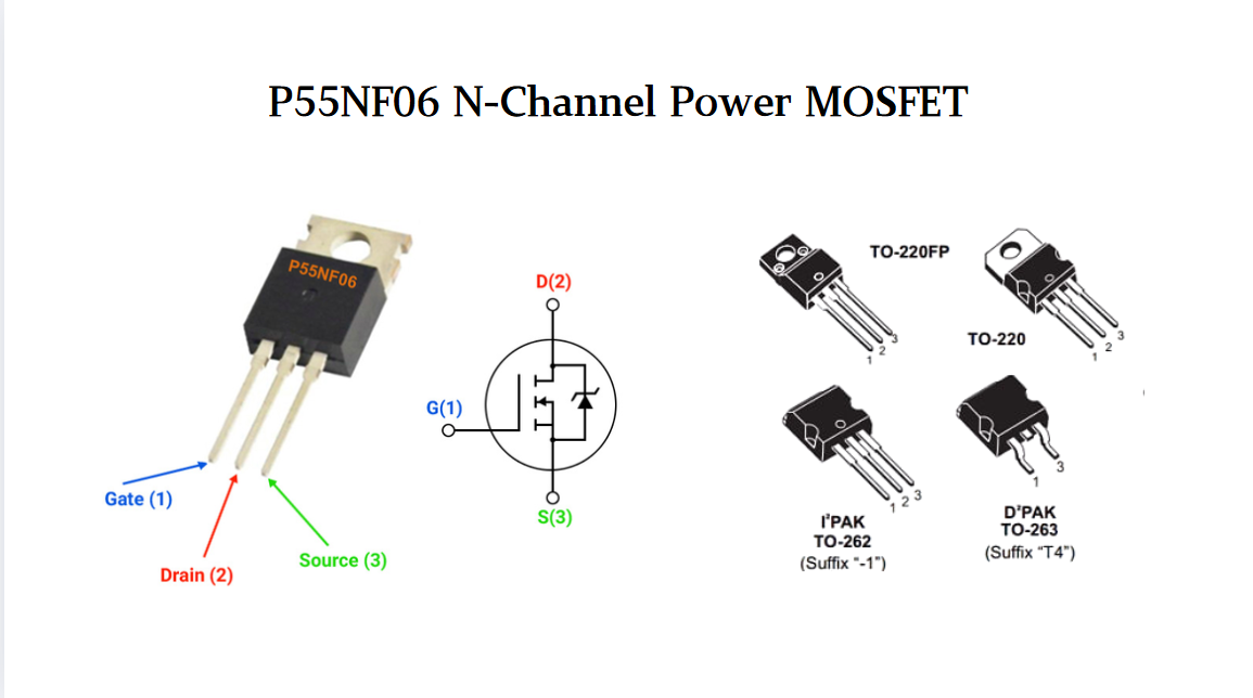
P55NF06 N-Channel Power MOSFET: Everything You Need To Know
In the vast landscape of semiconductor devices, MOSFETs (Metal - Oxide - Semiconductor Field - Effect Transistors) play a pivotal role, especially in power electronics. Among the numerous MOSFET models available, the P55NF06 stands out for its unique combination of features, making it suitable for a...
-
2025 / 07 / 23
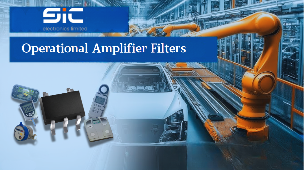
Operational Amplifier Filters: A Comprehensive Analysis from Fundamentals to Applications
In electronic systems, the purity and accuracy of signals directly determine the performance of devices. Electronic filters composed of operational amplifiers (op-amps) have become a "bridge" connecting original signals and valid information, thanks to their ability to precisely filter signal freque...
-
2025 / 07 / 19
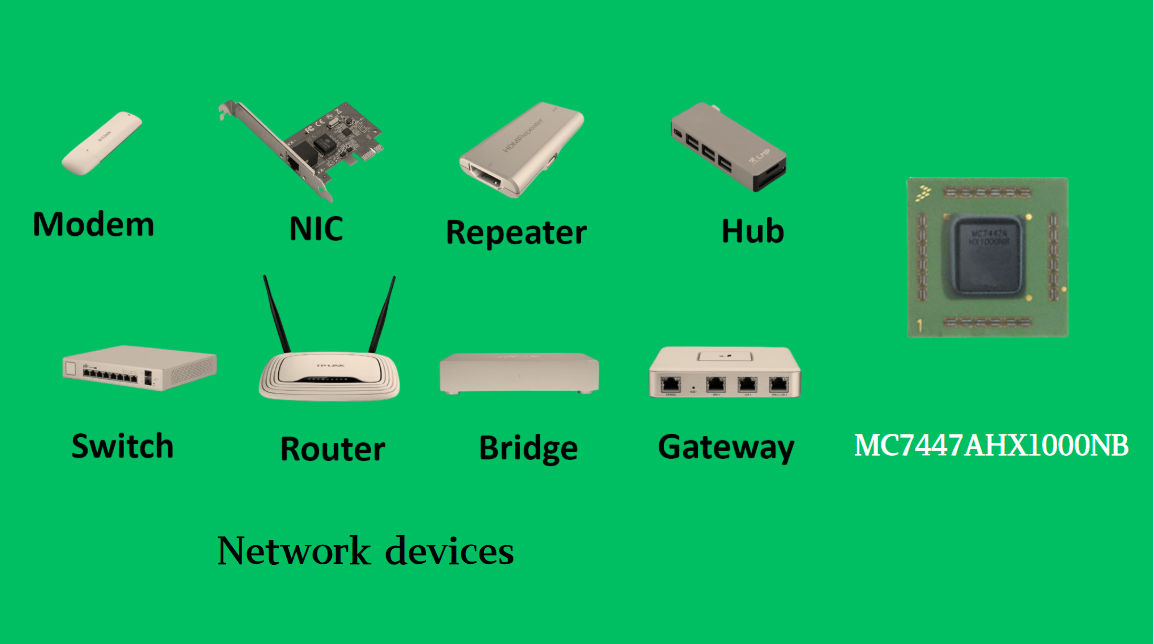
Broadcom BCM5714CKPB: Featrues,Applications,Datasheet And Advantages
When it comes to reliable, high-performance network connectivity in enterprise and industrial systems, the Broadcom BCM5714CKPB stands as a standout solution. This dual-port Gigabit Ethernet controller, developed by Broadcom—a leader in semiconductor innovation—combines robust features, versatile co...

-
2025 / 07 / 15
MC7447AHX1000NB: Technical Analysis and Applications of a High-Performance PowerPC Architecture Proc
In the field of embedded computing and network systems, the performance, energy efficiency, and compatibility of processors are often crucial to the success of a design. The MC7447AHX1000NB launched by NXP (formerly Freescale), as an important member of the MPC7447A series, has become an ideal choic...
-
2025 / 07 / 14
Nexperia Unveils New 1200V/20A SiC Schottky Diodes to Empower Efficient Industrial Power Innovations
Nexperia recently announced the addition of two new 1200V, 20A silicon carbide (SiC) Schottky diodes—PSC20120J and PSC20120L—to its power electronics portfolio, further expanding its product landscape in high-performance semiconductors. Specifically designed to address the increasingly stringent dem...

-
2025 / 07 / 09
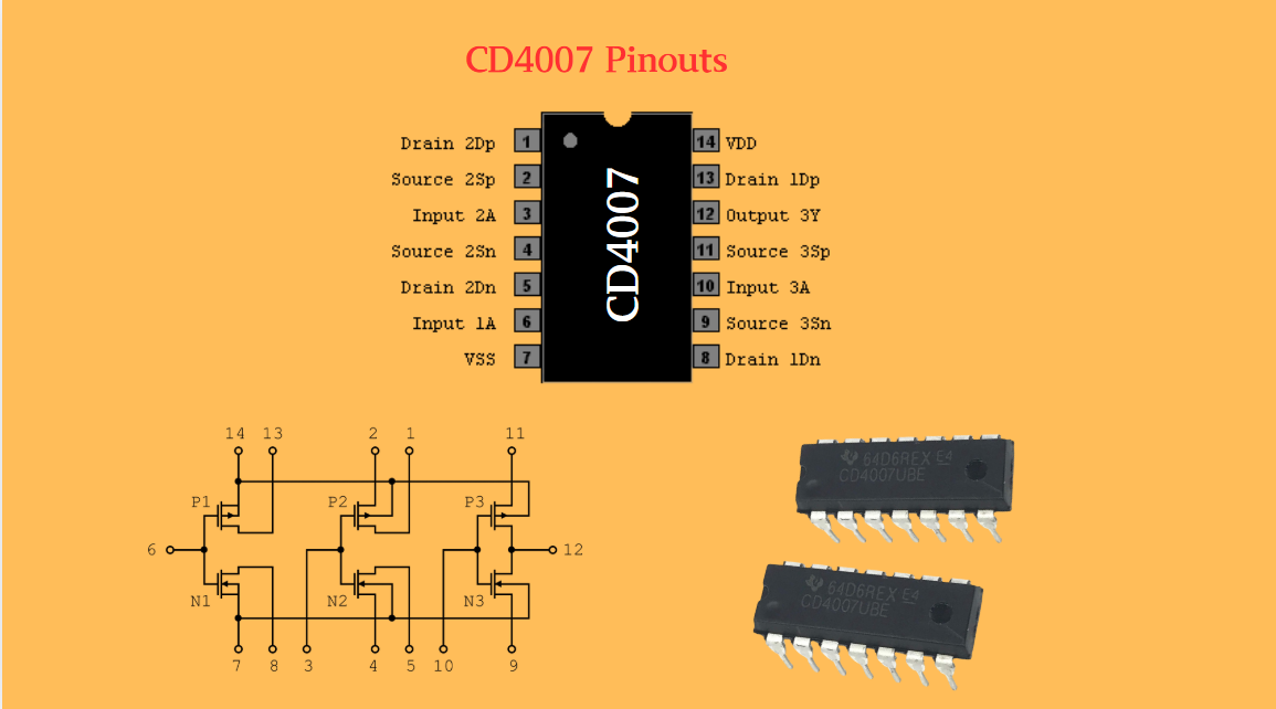
CD4007: A Comprehensive Analysis of a Multifunctional CMOS Integrated Circuit
In the field of modern electronic technology, CMOS (Complementary Metal-Oxide-Semiconductor) integrated circuits have become core components in digital and analog circuit design due to their low power consumption, high integration, and excellent compatibility. As a classic CMOS device, the CD4007 oc...
-
2025 / 07 / 07
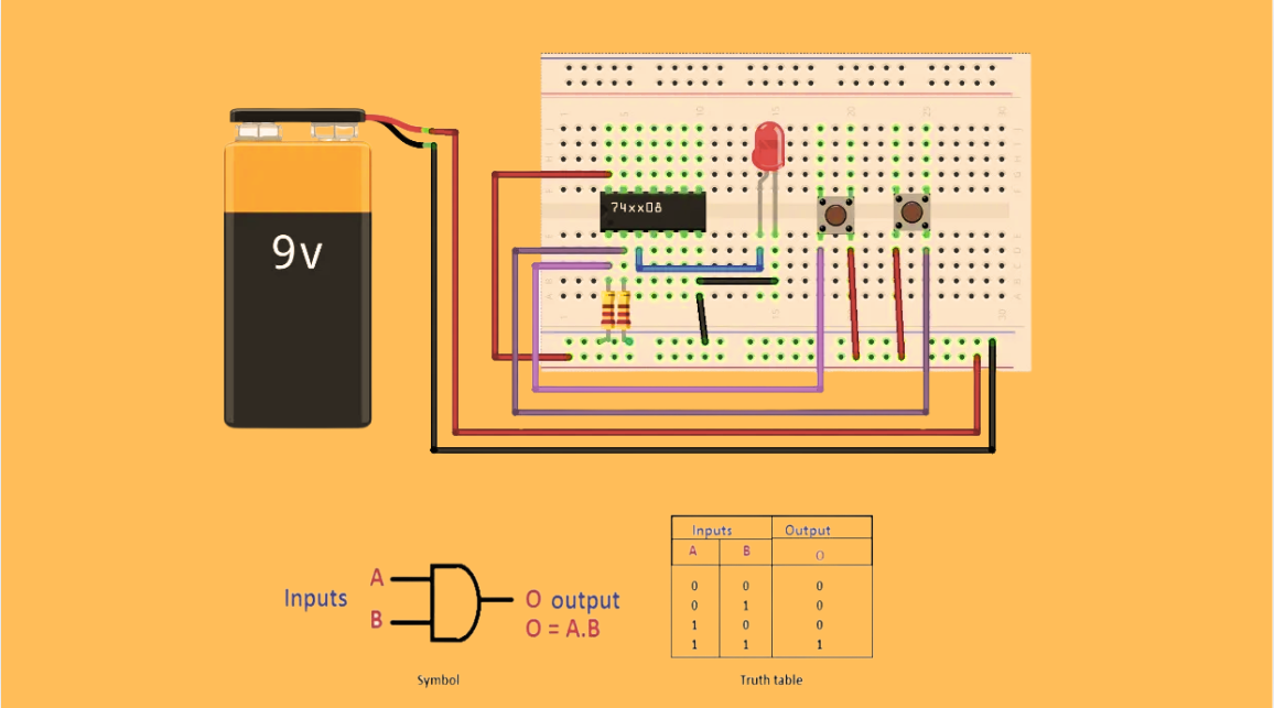
Understanding IC 7408: A Fundamental Component in Digital Logic Design
In the vast and intricate realm of digital electronics, integrated circuits (ICs) serve as the building blocks that enable the creation of complex and powerful systems. Among these, the IC 7408 holds a special place as a fundamental component in digital logic design. This article aims to provide a c...
-
2025 / 07 / 04
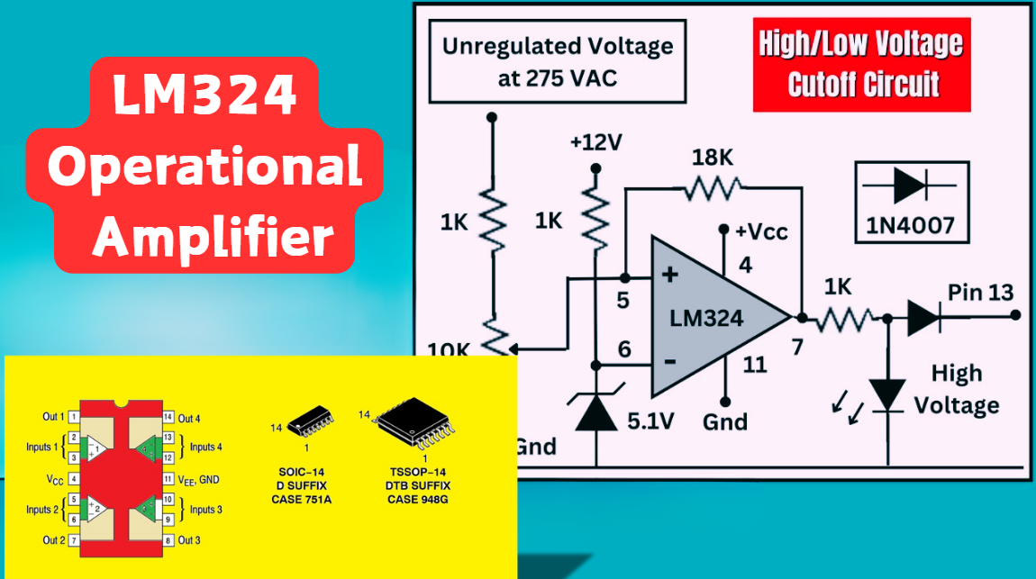
LM324 Operational Amplifier Comprehensive Guide: Pins, Applications, Packaging, and Datasheet
The LM324 is a low-cost integrated circuit featuring four independent operational amplifiers (op-amps), renowned for its wide voltage adaptability, low power consumption, and high reliability in industrial and consumer electronics. With a single-supply voltage range of 3V to 32V (or dual-supply rang...
-
2025 / 07 / 02
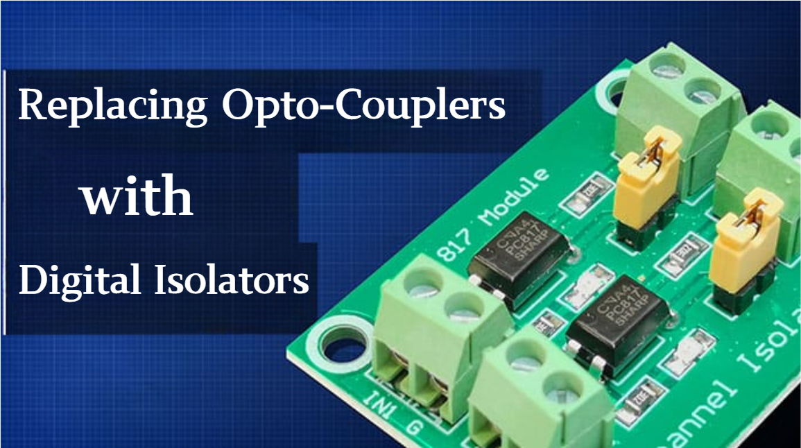
A Comprehensive Guide to Replacing Opto-Couplers with Digital Isolators: From Principles to Practice
In the ever-evolving landscape of electronic design, the transition from opto-couplers to digital isolators marks a pivotal shift in isolation technology. For decades, opto-couplers have been the cornerstone of electrical isolation in industrial control, medical devices, and power systems, relying o...

2000+
Daily average RFQ Volume

30,000,000
Standard Product Unit

2800+
Worldwide Manufacturers

15,000 m2
In-stock Warehouse
 Wishlist (0 Items)